
HDP/PECVD methods of fabricating stress nitride structures for field effect transistors, and field effect transistors so fabricated

a field effect transistor and stress nitride technology, applied in the direction of basic electric elements, electrical equipment, semiconductor devices, etc., can solve the problems of reducing achieve the effects of improving the performance and/or reliability of the device, uniform thickness, and enhanced chemical vapor depositing

Active Publication Date: 2007-05-03
SAMSUNG ELECTRONICS CO LTD +1
View PDF12 Cites 35 Cited by
  • Summary
  • Abstract
  • Description
  • Claims
  • Application Information

AI Technical Summary

Benefits of technology

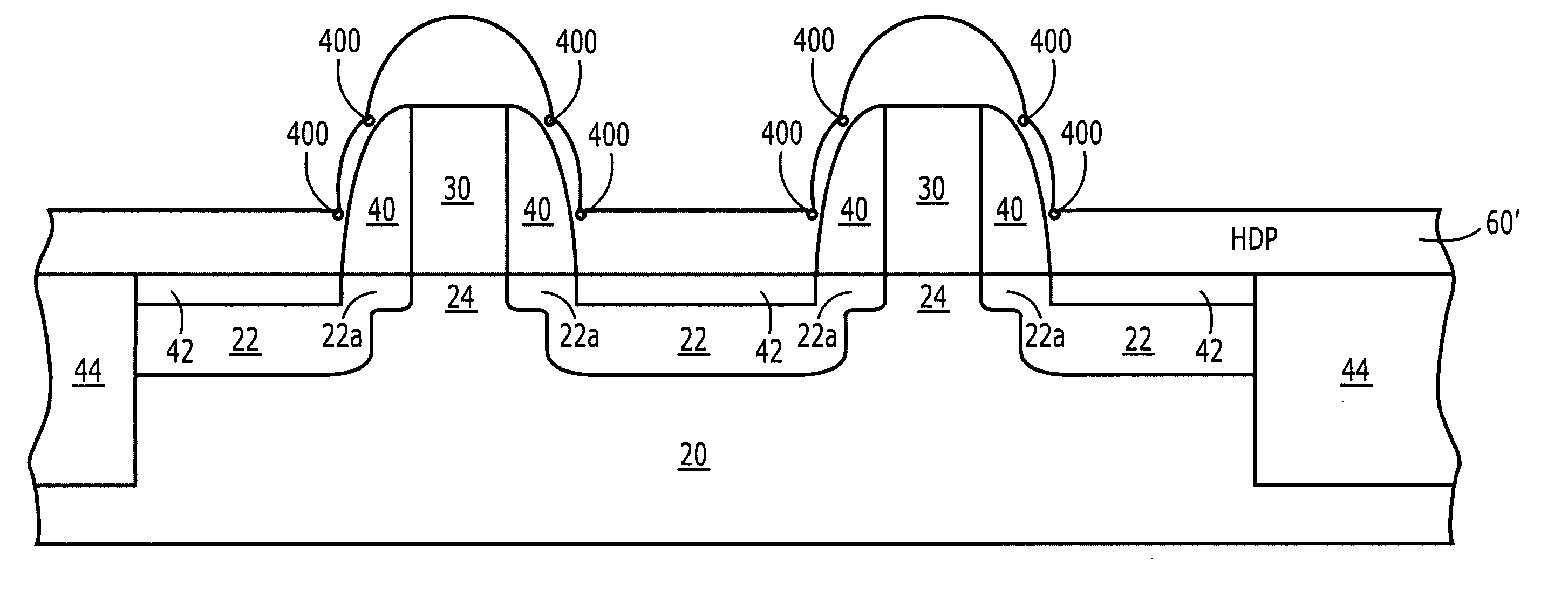
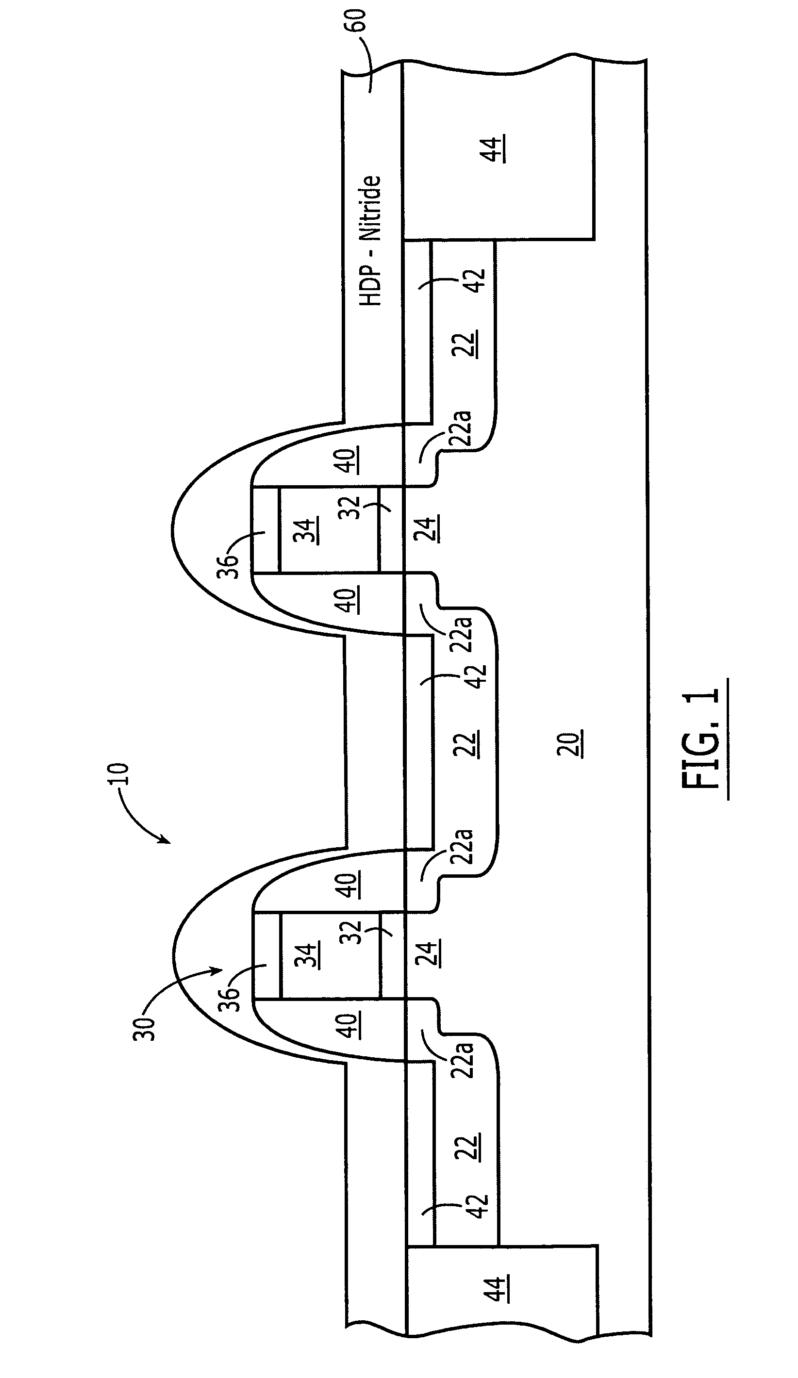
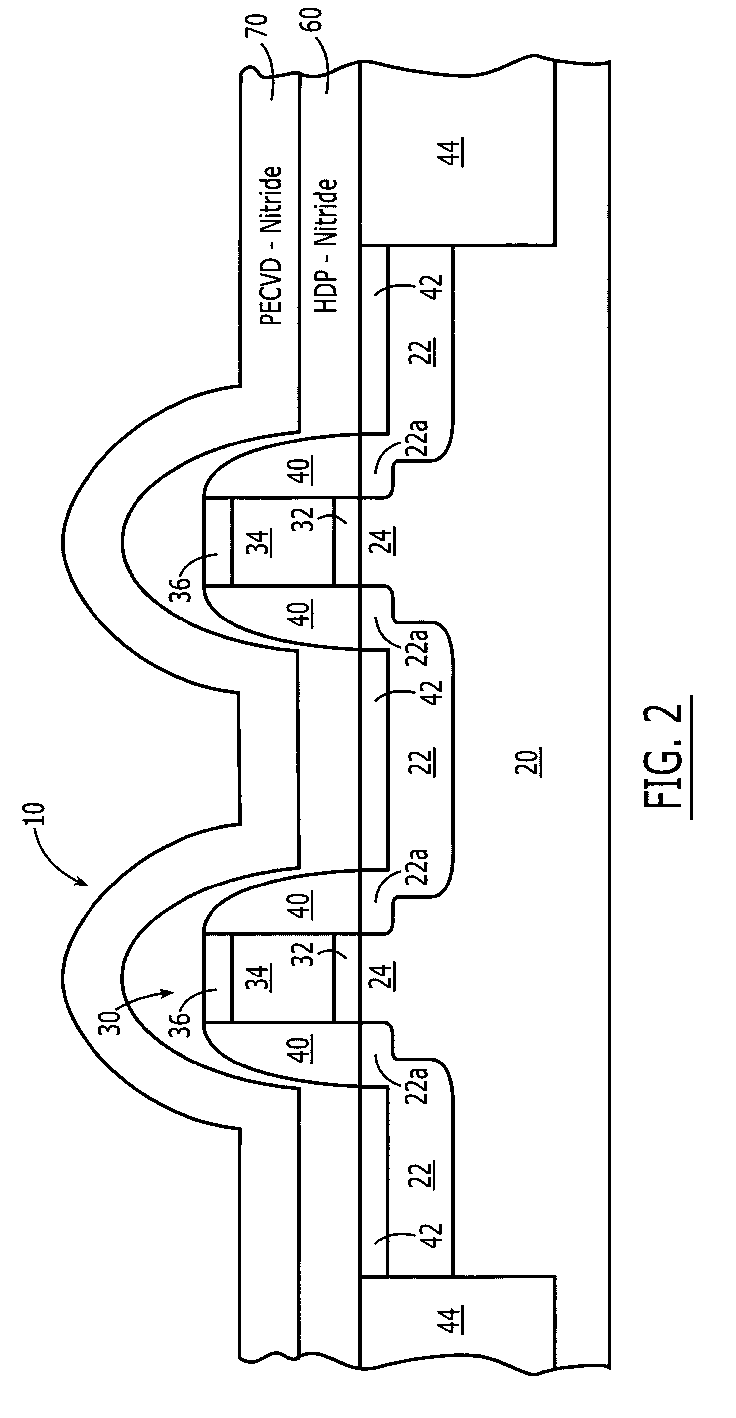
[0005] Stress nitride structures are fabricated, according to various embodiments of the present invention, by high density plasma (HDP) depositing a first stress nitride layer on an integrated circuit field effect transistor and then plasma enhanced chemical vapor depositing (PECVD) a second stress nitride layer on, and in some embodiments directly on, the first stress nitride layer. In some embodiments, HDP depositing the first stress nitride layer forms the first stress nitride layer thinner on the sidewall spacers than on source / drain regions of the field effect transistors thereof. Moreover, PECVD of the second stress nitride layer forms the second stress nitride layer more uniformly thick than the first stress nitride layer. In some embodiments, the second stress nitride layer is uniformly thick on the gate, sidewall spacer and source / drain regions.
[0006] In some embodiments, the first and second stress nitride layers are of about the same thickness on the gate and / or source / drain regions of the field effect transistor and, in other embodiments, the first and second stress nitride layers are both between about 300 Å and about 500 Å in thickness on the gate and / or source / drain regions of the field effect transistor. Moreover, in yet other embodiments, the field effect transistor is a P-channel field effect transistor, and the first and second stress nitride layers are both configured to apply compressive stress to a P-channel region of the P-channel field effect transistor. In still other embodiments, the first stress nitride layer is HDP deposited sufficiently thin so as to reduce, and in some embodiments avoid, foldover voids therein, but sufficiently thick such that the second stress nitride layer has reduced, and in some embodiments is free of, voids between adjacent transistor gates.
[0007] Stress nitride structures may be fabricated according to other embodiments of the present invention by non-conformally depositing a first stress nitride layer on, and in some embodiments directly on, the integrated circuit field effect transistor, such that the first stress nitride layer is thinner on a sidewall spacer of the field effect transistor than on the spaced apart source / drain regions thereof. A second stress nitride layer is conformally deposited on the first stress nitride layer, such that the second stress nitride layer is of more uniform thickness than the first stress nitride layer. As was described above, the first stress nitride layer may be fabricated by HDP and the second stress nitride layer may be formed by PECVD, with thickness ranges as described above.
[0008] Integrated circuit field effect transistors according to exemplary embodiments of the invention include a substrate, spaced apart source / drain regions in the substrate, an insulated gate on the substrate between the spaced apart source / drain regions and a sidewall spacer on a sidewall of the insulated gate. A first stress nitride layer is provided on the integrated circuit field effect transistor that is thinner on the sidewall spacer than on the spaced apart source / drain regions. A second stress nitride layer of relatively uniform thickness is provided on the first stress nitride layer. Thicknesses and / or fabrication processes as described above may be provided.

Problems solved by technology

Unfortunately, however, relatively thick stress nitride liners may include voids therein which can degrade the performance and / or reliability of the device.

Method used


Image

  • HDP/PECVD methods of fabricating stress nitride structures for field effect transistors, and field effect transistors so fabricated
  • HDP/PECVD methods of fabricating stress nitride structures for field effect transistors, and field effect transistors so fabricated
  • HDP/PECVD methods of fabricating stress nitride structures for field effect transistors, and field effect transistors so fabricated

Examples


Embodiment Construction

[0011] The invention will be described more filly hereinafter with reference to the accompanying drawings, in which example embodiments of the invention are shown. This invention may, however, be embodied in many different forms and should not be construed as limited to the example embodiments set forth herein. Rather, the disclosed embodiments are provided so that this disclosure will be thorough and complete, and will fully convey the scope of the invention to those skilled in the art. In the drawings, the size and relative sizes of layers and regions may be exaggerated for clarity unless express so defined herein. Moreover, each embodiment described and illustrated herein includes its complementary conductivity type embodiment as well. Like numbers refer to like elements throughout.

[0012] It will be understood that when an element or layer is referred to as being “on”, “connected to” and / or “coupled to” another element or layer, it can be directly on, connected or coupled to the...


PUM


Abstract

A stress nitride structure is formed on an integrated circuit field effect transistor by high density plasma (HDP) depositing a first stress nitride layer on the integrated circuit field effect transistor and then plasma enhanced chemical vapor depositing (PECVD) a second stress nitride layer on the first stress nitride layer. The first stress nitride layer is non-conformial and the second stress nitride layer is conformal. Related structures also are described.

Description

FIELD OF THE INVENTION [0001] This invention relates to integrated circuit field effect transistor fabrication methods and structures, and more particularly to methods of fabricating stress nitride structures for integrated circuit field effect transistors and structures formed thereby. BACKGROUND OF THE INVENTION [0002] Integrated circuit field effect transistors are widely used for consumer, commercial and other applications. As is well known to those having skill in the art, integrated circuit field effect transistors include spaced apart source / drain regions in a substrate and a channel region in the substrate between the spaced apart source / drain regions. An insulated gate is provided on the channel region between the spaced apart source / drain regions. The insulated gate may include a sidewall spacer on a sidewall thereof. [0003] It is known that the carrier mobility in the channel region of a field effect transistor can be changed by applying stress to the channel region. Tens...

Claims


Application Information

Patent Timeline
Patent Type & Authority Applications(United States)
IPC IPC(8): H01L21/336H01L29/94
CPCH01L21/823412H01L21/823425H01L21/823468H01L21/823807H01L21/823864H01L29/7843H01L21/823814
Inventor KIM, JUNJUNGPARK, JAE-EUNKU, JA-HUMYANG, DAEWON
Owner SAMSUNG ELECTRONICS CO LTD
Learn More