Clock forming method for semiconductor integrated circuit and program product for the method

a technology of integrated circuits and clocks, which is applied in the direction of pulse techniques, generating/distributing signals, instruments, etc., can solve the problems of clock skew increase on an actual device, difficulty in accurately and correctly supplying clocks to all sequential, etc., and achieve the effect of improving the on-chip variability resistan

Inactive Publication Date: 2007-04-26
RENESAS ELECTRONICS CORP
View PDF5 Cites 9 Cited by
  • Summary
  • Abstract
  • Description
  • Claims
  • Application Information

AI Technical Summary

Benefits of technology

[0014] The present invention has been developed to solve the above-described problems, and therefore it is an object of the present invention to provide a provide a cl...

Problems solved by technology

It is difficult to supply a clock accurately and correctly to all sequential elements of a large scale semiconductor integrated circuit (LSI).
Therefore, if the data connection channels are not uniform, a difference occurs between an assumed delay va...

Method used


Image

  • Clock forming method for semiconductor integrated circuit and program product for the method
  • Clock forming method for semiconductor integrated circuit and program product for the method
  • Clock forming method for semiconductor integrated circuit and program product for the method

Examples


first embodiment

[0025] A clock forming method for a semiconductor integrated circuit according to the first embodiment of the present invention will be described. The clock forming method described below is a method of performing clock tree synthesis (hereinafter referred to as “CTS”) after dividing a circuit region (grouping).

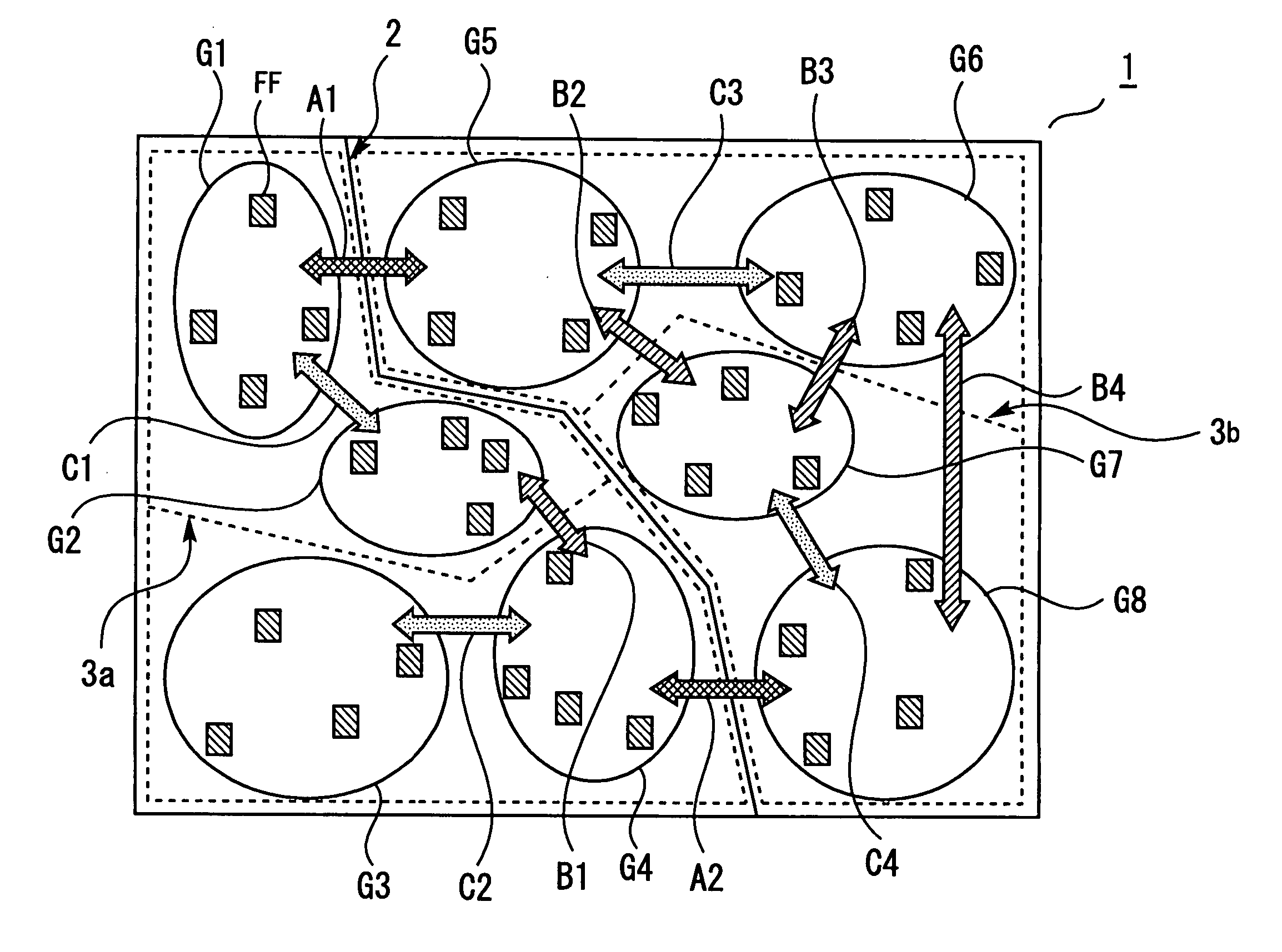
[0026] A method of dividing a circuit region into groups of regions will first be described. As shown in FIG. 1, a multiplicity of flip-flops (hereinafter referred to “FF”) exit in a circuit region 1. As a standard method of dividing into groups regions, a method of grouping FFs into groups of equal numbers of FFs or a method of dividing an area into equal parts may be used. An example of grouping by dividing a region into equal parts for equal number of FFs will be described below.

[0027] As shown in FIG. 1, each of regions G1 to G8 contains four FFs. Connection channels for data transfer between certain regions (hereinafter referred to as “data connection channel”) exist b...

second embodiment

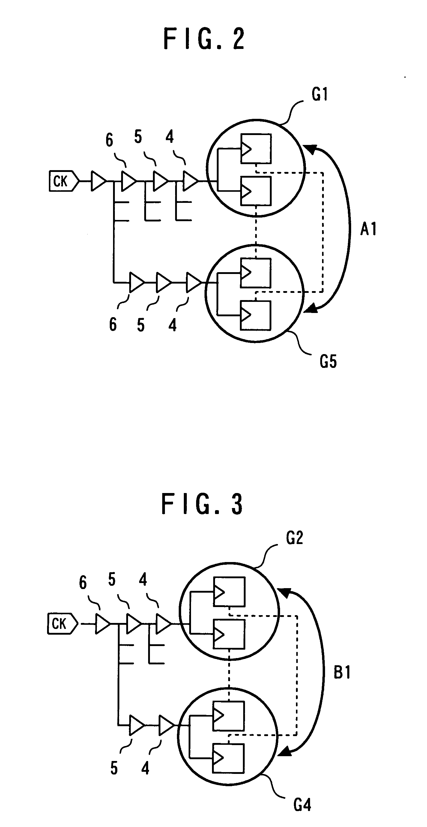
[0038] A clock forming method for a semiconductor integrated circuit according to the second embodiment of the present invention will be described. The second embodiment will be described with respect to points of difference from the first embodiment. In the above-described grouping method in the first embodiment, grouping is performed so that the number of data connection channels intersected by a boundary is minimized. With respect to grouping by this method, dividing into a group of regions G1 to G4 and a group of regions G5 to G8 as shown in FIG. 4 is conceivable.

[0039] In this case, the number of data connection channels intersected by the boundary 2 is two, the minimum number. However, the regions G5 to G8 extend largely along the periphery of the circuit region 1. Therefore, if CTS is executed in the state shown in FIG. 4, the clock delay is increased. An increase in clock delay leads to a reduction in on-chip-variation resistance. For this reason, dividing such as described...


PUM


Abstract

Regions G1 to G8 each including a predetermined number of flip-flops (FF) are divided into two groups. This dividing is performed so that the number of data connection channels intersected by a boundary is minimized. In the case of intersection of two data connection channels (A1, A2), the number of data connection channels intersected by the boundary is two, the minimum number. After grouping of all the regions (G1 to G4, G5 to G8), clock tree synthesis (CTS) is performed. If clock forming is performed in this way, the increase in clock skew on an actual device can be limited and on-chip variation resistance can be increased.

Description

BACKGROUND OF THE INVENTION [0001] 1. Field of the Invention [0002] The present invention relates to a clock forming method for a semiconductor integrated circuit and a program product for the method, and more particularly, to the method and the program product for the improved on-chip-variation resistance. [0003] 2. Background Art [0004] It is difficult to supply a clock accurately and correctly to all sequential elements of a large scale semiconductor integrated circuit (LSI). In ordinary cases, a clock is supplied to different portions at different times. The difference between times at which a clock is supplied is called a clock skew. With the increase in packaging density and the increase in degree of integration of LSIs, a need has arisen to reduce clock skews of a clock applied to different portions. Clock skews are produced mainly at the design stage. Therefore, clock skew control with high accuracy is required when a clock is formed. [0005] In Japanese Unexamined Patent Pub...

Claims


Application Information

Patent Timeline
IPC IPC(8): G06F17/50
CPCG06F17/5045G06F2217/62G06F30/396G06F30/30
Inventor KOMODA, MICHIO
Owner RENESAS ELECTRONICS CORP
Why Eureka
Try Eureka