
Light emitting apparatus, method of manufacturing light emitting apparatus, and electronic apparatus

Active Publication Date: 2007-04-05
SEIKO EPSON CORP
View PDF3 Cites 29 Cited by
  • Summary
  • Abstract
  • Description
  • Claims
  • Application Information

AI Technical Summary

Benefits of technology

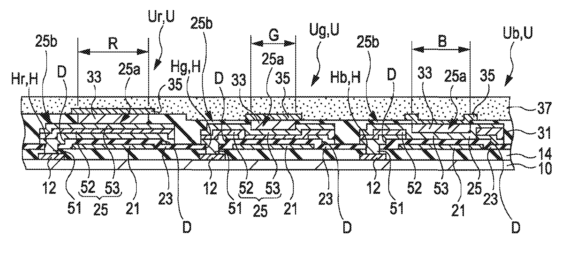
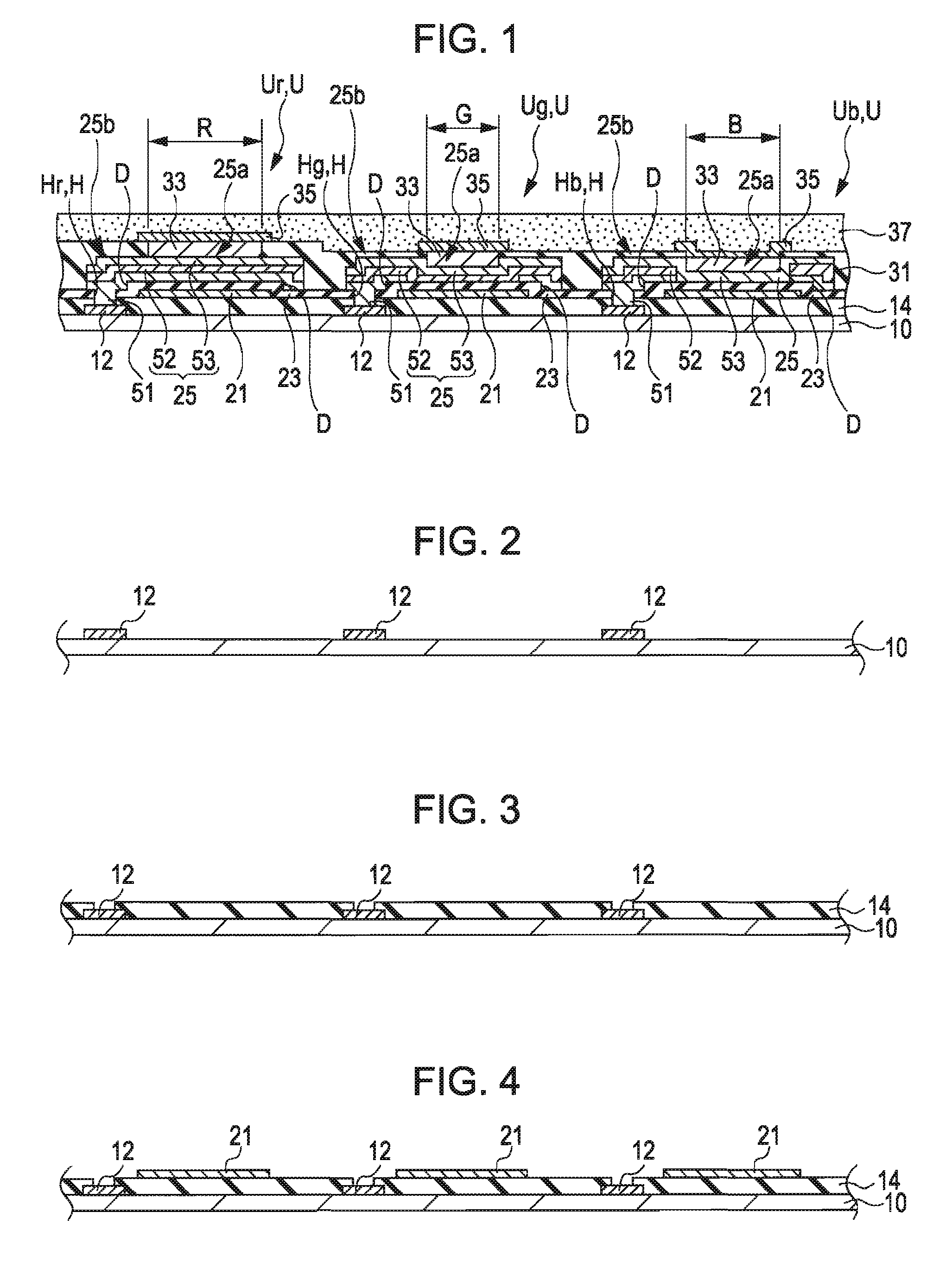
[0010] In such a light emitting apparatus, if the number of the stacked electrode layers in the electrode portion of each of the first unit devices is smaller than the number of the stacked electrode layered in the electrode portion of each of the second unit devices, when the electrode layers which are to be the pixel electrodes of the first unit devices are formed, the electrode layers corresponding to the electrode portions of the second unit devices may be removed by initial patterning. However, in the light emitting apparatus according to the invention, since the pixel electrode of the second unit device is formed by stacking the electrode layer corresponding to the electrode and connection portions and the electrode layer corresponding to the connection portion, when the electrode layers constituting the pixel electrode constituting the first unit device is patterned, the electrode layer corresponding to the connection portion of the second unit device may not be removed. Therefore, in a process of manufacturing the light emitting apparatus according to the invention, a surface of the substrate corresponding to the connection portion is not exposed to an etchant used for pattering the electrode layer. For example, when a contact hole is formed to expose a wire line on a surface of the substrate corresponding to the connection portion, the contact hole is not exposed to the echant used for pattering the electrode layer. As a result, in the light emitting apparatus according to the invention, it is possible to effectively prevent the etchant used for pattering the electrode layer from deteriorating electrical characteristics of the light emitting apparatus.
[0035] According to the electronic apparatus, the electronic apparatus can include a light emitting apparatus capable of obtaining high reliability in electrical connection between the wire lines and the pixel electrodes and stabilized electrical characteristics.

Problems solved by technology

In such a light emitting apparatus, since light emitted from the light emitting layer has a wide spectrum peak width and low intensity, there is a problem in that it is difficult to secure sufficient color reproducibility in a case where the light emitting apparatus is used as a display apparatus.
When first electrodes included in unit devices having a large thickness are patterned, contact holes constituting unit devices including first electrode having a small thickness are exposed to an etchant, so that there may be deterioration in electric characteristics of the light emitting apparatus.

Method used


Image

  • Light emitting apparatus, method of manufacturing light emitting apparatus, and electronic apparatus
  • Light emitting apparatus, method of manufacturing light emitting apparatus, and electronic apparatus
  • Light emitting apparatus, method of manufacturing light emitting apparatus, and electronic apparatus

Examples


modified examples

[0096] The aforementioned embodiment may be modified in various manners. The examples of the modifications are as follows. In addition, the examples may be used in combination thereof.

[0097] (1) Although the protective film 23 is formed to cover the light reflecting layer 21 in the aforementioned embodiment, the protective film 23 may not be employed.

[0098] (2) Although the elements constituting the unit devices U corresponding to colors of emitted light are formed to be separated from each other in the aforementioned embodiment, the elements may be formed continuously over the unit devices corresponding to the colors of emitted light. For example, at least one functional layer of the light emitting members 33 or the second electrode 35 may be continuously distributed over all the unit devices U. Although the light emitting layer is continuously formed over all the unit devices, the unit devices U can emit light in different colors by suitably selecting the resonance wavelengths o...


PUM


Abstract

A light emitting apparatus is provided. The light emitting apparatus has a plurality of unit devices including, on a substrate, a reflecting layer, a semi-transmitting semi-reflecting layer, a light emitting layer disposed between the light reflecting layer and the semi-reflecting layer, and a light transmitting pixel electrode disposed between the light reflecting layer and the semi-reflecting layer, a plurality of the unit devices including light emitting regions provided with resonator structures, so that a plurality of the unit devices include first and second unit devices of which resonance wavelengths of the resonator structures are different from each other, wherein the pixel electrode includes an electrode portion disposed in the light emitting region and a connection portion connected to a wire line, wherein the pixel electrode of each of the first unit devices is constructed by stacking a plurality of electrode layers corresponding to the electrode portion and the connection portion, wherein the pixel electrode of each of the second unit devices is constructed by stacking at least electrode layers corresponding to the electrode layer and the connection layer and an electrode layer corresponding to the connection portion, and wherein the number of the stacked electrode layers in the electrode portion of each of the first unit devices is smaller than the number of the stacked electrode layered in the electrode portion of each of the second unit devices.

Description

BACKGROUND [0001] 1. Technical Field [0002] The present invention relates to a light emitting apparatus, a method of manufacturing a light emitting apparatus, and an electronic apparatus. [0003] 2. Related Art [0004] In the related art, there is proposed a light emitting apparatus where devices (hereinafter, referred to a unit device) constructed by interposing a light emitting layer made of a light emitting material such as an organic EL (Electro Luminescent) material between first and second electrodes are arrayed on a substrate. In such a light emitting apparatus, since light emitted from the light emitting layer has a wide spectrum peak width and low intensity, there is a problem in that it is difficult to secure sufficient color reproducibility in a case where the light emitting apparatus is used as a display apparatus. [0005] In order to solve the problem, for example, In WO2001039554, disclosed is a construction where resonator structures for resonating the light emitted from...

Claims


Application Information

Patent Timeline
IPC IPC(8): H01L29/06
CPCH01L27/3211H01L51/5203H01L51/5237H01L51/5265H10K59/351H10K59/805H10K59/876H10K50/852H10K50/805H10K50/841
Inventor MIYATA, TAKASHIEGUCHI, TSUKASAIWASHITA, TAKAHIRO
Owner SEIKO EPSON CORP
Learn More