Semiconductor memory device for adjusting impedance of data output driver

Active Publication Date: 2007-03-29
SK HYNIX INC
View PDF9 Cites 65 Cited by
  • Summary
  • Abstract
  • Description
  • Claims
  • Application Information

AI Technical Summary

Benefits of technology

[0073] It is, therefore, an object of the present invention to provide a semiconductor memory device fo

Problems solved by technology

However, sometimes, the pull-up or the pull-down impedance applied to the DQ PAD 50 may be variable because of several problems occurred in the fabricated semiconductor memory device.

Method used


Image

  • Semiconductor memory device for adjusting impedance of data output driver
  • Semiconductor memory device for adjusting impedance of data output driver
  • Semiconductor memory device for adjusting impedance of data output driver

Examples


Embodiment Construction

[0089] Hereinafter, a synchronous semiconductor memory device in accordance with the present invention will be described in detail referring to the accompanying drawings.

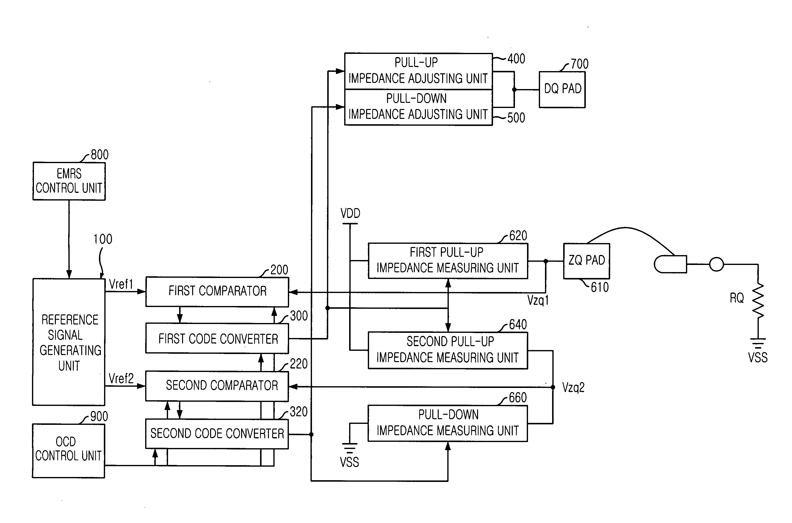
[0090]FIG. 7 is a block diagram showing a device for performing the OCD calibration control of a semiconductor memory device in accordance with an embodiment of the present invention.

[0091] As shown, the device for performing the OCD calibration control in accordance with the embodiment of the present invention includes a reference signal generating unit 100, a pull-up comparing unit, a pull-down comparing unit, a pull-up impedance adjusting unit 400, a pull-down impedance adjusting unit 500, a test pad (hereinafter, referring to a ZQ PAD) 600, a first pull-up impedance measuring unit 620, a second pull-up impedance measuring unit 640, a pull-down impedance measuring unit 660, a data input / output (I / O) pad (hereinafter, referring to a DQ PAD) 700, a reference signal control unit 800 and an impedance control unit 9...


PUM


Abstract

An apparatus for comparing inputted signals by removing an offset voltage during adjusting an output impedance of a semiconductor memory device, includes a voltage comparator for comparing a first input signal applied to its positive input node with a second input signal applied to its negative input node to output a first output signal to its positive output node and its second output signal to a negative output node; a switched capacitive unit for removing an offset voltage occurred in the positive input node, the negative input node, the positive output node and the negative output node of the voltage comparator; and a latch unit for latching the first output signal and the second output signal.

Description

FIELD OF THE INVENTION [0001] The present invention relates to a semiconductor memory device; and, more particularly, to a semiconductor memory device for adjusting an output impedance of an output driver. DESCRIPTION OF RELATED ARTS [0002] A dynamic random access memory (DRAM) has been improved continuously to increase its operational speed. Synchronizing an internal clock signal with an external clock signal is one of methods to improve the operational speed of the DRAM. The DRAM operating in synchronization with the external clock signal is called a synchronous DRAM (SDRAM). [0003] The SDRAM performs a data access operation in synchronization with a rising edge of the external clock signal. That is, the SDRAM can perform the data access operation once within one cycle of the external clock signal. Such an SDRAM that performs the data access operation once within one cycle of the external clock signal is particularly called a single data rate (SDR) SDRAM. [0004] However, the SDR S...

Claims


Application Information

Patent Timeline
IPC IPC(8): G11C7/06
CPCG11C7/1048G11C7/1051G11C7/106G11C7/1069G11C11/4093G11C2207/2254G11C29/022G11C29/028G11C29/50008G11C2207/105G11C29/02G11C7/10G11C11/4096
Inventor KIM, KYUNG-HOON
Owner SK HYNIX INC
Why Eureka
Try Eureka