Substrate processing apparatus and substrate processing method

a substrate processing and processing apparatus technology, applied in the direction of photomechanical apparatus, instruments, photosensitive materials, etc., can solve the problems of affecting the yield affecting the effect of the whole processing apparatus, and reducing the yield of the development processing, so as to achieve the effect of increasing the effect and reducing the yield

Inactive Publication Date: 2007-03-22
ITO YOSHITAKE
View PDF3 Cites 1 Cited by
  • Summary
  • Abstract
  • Description
  • Claims
  • Application Information

AI Technical Summary

Benefits of technology

[0010] Further, since the developing solution is supplied to a substrate in a cup to continue the development while exhausting the downflow with controlled temperature and moisture from the cup, the downflow has a significant effect on the developing solution on the substrate. There is, therefore, a fear that the developing solution on the substrate may spill as a result of the increased effect of the downflow, resulting in a factor for decreasing the yield in the development processing.
[0016] The present invention allows exhaust primarily from the first peripheral region around the substrate undergoing processing, and further from the second peripheral region between the first peripheral region and the substrate. Therefore, the present invention enables reduced effects of currents of air on a processing solution, for example, developing solution on a processing surface of the substrate, further enables the developing solution used in development to properly act on the exposed resist on the substrate, and thus enhances the uniformity in the processing on the substrate and improves the yield in the processing on the substrate.

Problems solved by technology

Since the substrate is placed near an inject opening of the downflow with controlled temperature and moisture after supplying a developing solution to the substrate, there is a possibility that the developing solution on the substrate may spill as a result of the increased effect of the downflow, resulting in a decrease in the yield in the development processing.
There is, therefore, a fear that the developing solution on the substrate may spill as a result of the increased effect of the downflow, resulting in a factor for decreasing the yield in the development processing.
Then, the mists are generated in the processing chamber when the solution(s) dries, or the solutions adhered to the back of the substrate become mists in a subsequent processing chamber or during carriage of the substrate, and thus the whole processing apparatus is polluted.
This results in factors for decreasing not only the yield in the development processing, but also the yield in the entire substrate processing.

Method used


Image

  • Substrate processing apparatus and substrate processing method
  • Substrate processing apparatus and substrate processing method
  • Substrate processing apparatus and substrate processing method

Examples


Embodiment Construction

[0040] Embodiments of the present invention will be described below specifically with reference to the accompanying drawings.

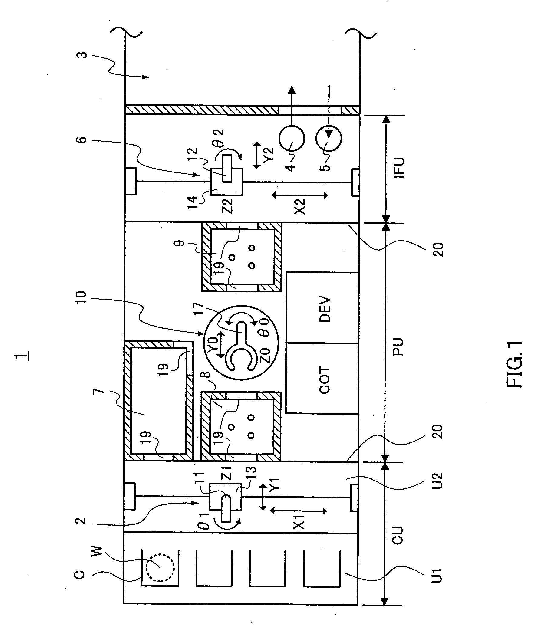
[0041]FIG. 1 is a schematic plan view showing an entire structure of a coating / developing apparatus as a solution processing apparatus, for example, resist processing apparatus according to one embodiment of the invention.

[0042] A resist processing apparatus 1 has in its primary portion a cassette unit section CU having a cassette mount section U1 enabling itself to mount a plurality of cassettes C thereon where each cassette enables itself to store a plurality of substrates, for example, semiconductor wafers W, and a substrate carrying in / out mechanism section U2 having a substrate carrying in / out mechanism 2 enabling each semiconductor wafer W to be carried in or out of a cassette C in the cassette mount section U1 on a sheet basis. An interface unit IFU section has a providing section 4 that provides each semiconductor wafer W on a sheet basis to another ...


PUM

PropertyMeasurementUnit
concentrationaaaaaaaaaa
temperatureaaaaaaaaaa
yieldaaaaaaaaaa

Abstract

A substrate processing apparatus has at least one of a developing processing apparatus that supplies a developing solution as a processing solution to a non-processed substrate to process and a resist coating processing apparatus that supplies a resist solution as a processing solution to the non-processed substrate. A transfer mechanism enables the non-processed substrate to be transferred to the developing processing apparatus and / or the resist coating processing apparatus. In a substrate processing method processes, an exposed resist is developed on a processing surface of the non-processed substrate inside a cup mechanism of the developing processing apparatus, and a resist solution is supplied to the processing surface of the non-processed substrate inside a cup mechanism of a resist coating processing apparatus. the non-processed substrate is transferred to the developing processing apparatus or the resist coating processing apparatus.

Description

[0001] This is a continuation application of Ser. No. 11 / 337,643 filed on Jan. 24, 2006, which is a continuation application of Ser. No. 10 / 622,796 filed on Jul. 21, 2003, the subject matter of which is incorporated by reference herein.BACKGROUND OF THE INVENTION [0002] 1. Field of the Invention [0003] The present invention relates to a substrate processing apparatus and a substrate processing method. [0004] 2. Description of the Related Art [0005] It is generally known to use techniques of photolithography using photoresist in forming electronic materials such as substrates, for example, semiconductor wafers. An example of the techniques is disclosed in Japanese Laid-Open Patent Publication No. H02-296316. [0006] The technique discloses a paddle development scheme as development processing. During the progress of development on a substrate, instead of holding the substrate on a rotating stage movable upwardly and downwardly, the substrate is supported by a ring supporting frame. Th...

Claims


Application Information

Patent Timeline
Patent Type & Authority Applications(United States)
IPC IPC(8): G03F7/26H01L21/027G03F7/30
CPCG03F7/3021H01L21/67017H01L21/6875H01L21/68742H01L21/68735H01L21/027
Inventor ITO, YOSHITAKE
Owner ITO YOSHITAKE
Why Eureka
Try Eureka