Clock distribution circuit
a clock distribution and circuit technology, applied in the field of circuits, can solve the problems of limited clock tree, load capacity which can be driven by a single inverter, and increase the load capacity of the clock tr
- Summary
- Abstract
- Description
- Claims
- Application Information
AI Technical Summary
Benefits of technology
Problems solved by technology
Method used
Image
Examples
first embodiment
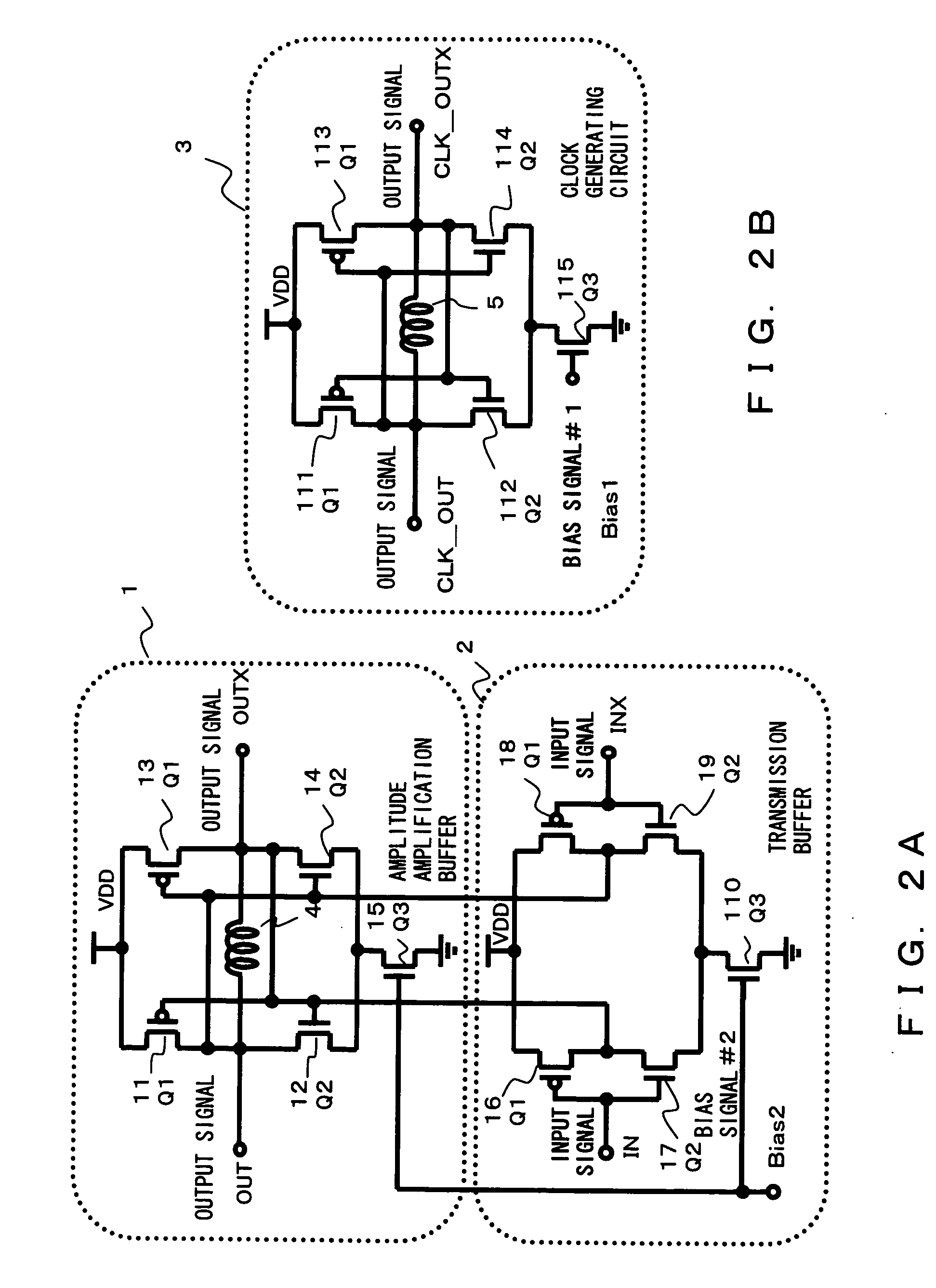
[0041]FIG. 2 shows an example configuration of a clock distribution circuit according to the present invention. FIG. 2A is a diagram showing an amplitude amplification buffer circuit 1 and a transmission buffer circuit 2. FIG. 2B is a diagram showing a clock generating circuit.
[0042] The amplitude amplification buffer circuit 1 shown in FIG. 2A is composed of transistors. For example, it comprises a first MOSFET_Q1 (11 and 13), a second MOSFET Q2 (12 and 14), a third MOSFET_Q3 (15) and an inductor 4. Here, the first MOSFET is a P-channel MOSFET (P-channel metal-oxide semiconductor), hereinafter referred to as Q1. In addition, the second and third MOSFETs are N-channel MOSFETs (N-channel metal-oxide semiconductor), hereinafter referred to as Q2 and Q3 respectively.
[0043] The sources of Q1_11 and Q1_13 are connected to the power supply (VDD). The drain of Q1_11 and the drain of Q2_12 are connected to the output terminal OUT, as is one terminal of the inductor 4. In addition, the gat...
second embodiment
[0063] Furthermore, as shown in FIG. 4, the clock generating circuit 3 can be configured using the same topology as the above-mentioned amplitude amplification buffer 1 and the transmission buffer 2.
[0064] A clock generating circuit 3 such as that described in FIG. 2(b) may be employed. The buffer 31 in FIG. 4 comprises Q1_111 and Q2_112 and the buffer 32 comprises Q1_113 and Q2_114. In other words, they are configured with P and N topologies. The power supplies 33 and 34 are Q3_115 shown equivalently.
[0065] In addition, although this will be described hereafter, the bias signal #1 for control of the bias in the clock generating circuit 3 does not use the same bias signal as the bias signal #2.
[0066] Here, the inductance 5 in the clock generating circuit 3 functions to amplify the amplitude. The capacitances 35 and 36 adjust the clock frequency. The capacitances 35 and 36 can be configured to enable variability.
[0067] In addition, the amplitude amplification buffer 1 does not os...
third embodiment
[0073] In the circuit according to a third embodiment, as shown in FIG. 5, the bias signal #2 of the circuit according to the second embodiment is generated by a common-mode feedback circuit 41.
[0074] The common-mode feedback circuit 41 (hereinafter referred to as the CMFB circuit) monitors the common voltage of output terminals OUT and OUTX. The CMFB circuit generates the bias signal #2 when the monitored voltage differs from a reference input voltage. The reference potential can be applied directly from an external source or can be generated in an internal circuit. In addition, although inputted by extending wiring the output terminals OUT and OUTX to the CMFB circuit 41 in the above diagram, the common-mode potential of OUT and OUTX can be generated by other methods, as well. In the CMFB circuit 41 in FIG. 6, the source of P-channel MOSFET 56 is connected to the power supply (VDD).
[0075] The gate of P-channel MOSFET 51 and the gate of N-channel MOSFET 52 are connected to the in...
PUM
 Abstract
Description
Claims
Application Information
 - R&D
- Intellectual Property
- Life Sciences
- Materials
- Tech Scout
- Unparalleled Data Quality
- Higher Quality Content
- 60% Fewer Hallucinations
Browse by: Latest US Patents, China's latest patents, Technical Efficacy Thesaurus, Application Domain, Technology Topic, Popular Technical Reports.
© 2025 PatSnap. All rights reserved.Legal|Privacy policy|Modern Slavery Act Transparency Statement|Sitemap|About US| Contact US: help@patsnap.com


