
Ald metal oxide deposition process using direct oxidation

a metal oxide and direct oxidation technology, applied in the direction of coatings, chemical vapor deposition coatings, metallic material coating processes, etc., can solve the problems of not addressing the removal of carbon from metal compounds produced from metal organic compounds, trace amounts of carbon in the deposited film,

Inactive Publication Date: 2007-03-15
APPLIED MATERIALS INC
View PDF98 Cites 440 Cited by
  • Summary
  • Abstract
  • Description
  • Claims
  • Application Information

AI Technical Summary

Benefits of technology

This method achieves the deposition of uniform, carbon-free metal oxide films, suitable for high-k gate dielectric layers, by controlling processing conditions and using a pulsed atomic layer deposition process, significantly improving film uniformity and reducing carbon content.

Problems solved by technology

Deposition of metal compounds from metal organic compounds typically results in trace amounts of carbon in the deposited film.
Although ALD enhances molecular reactions at the surface of the substrate between the metal organic precursors and reactive gases, the process temperatures and reaction times used for ALD typically do not reduce the carbon content below detectable limits.
However, the reference does not address removal of carbon from metal compounds produced from metal organic compounds.

Method used


Image

  • Ald metal oxide deposition process using direct oxidation
  • Ald metal oxide deposition process using direct oxidation
  • Ald metal oxide deposition process using direct oxidation

Examples


examples

[0037] Hafnium oxide films were deposited at a chamber pressure of 4 Torr by pulsing TDEAH in a nitrogen carrier for 10 seconds. The chamber was then purged with a pulse of a nitrogen gas for 10 seconds. Next, reactive oxygen and an argon carrier (Ar / O* ratio=1:2) was pulsed to the chamber for 10 seconds. Once the reactive gas / carrier pulse was terminated, a second pulse of nitrogen gas was introduced into the chamber for ten seconds to complete the cycle. This process was repeated for 40 cycles with substrate temperatures ranging from 150° C. to 325° C. The resulting hafnium oxide films were tested for WIW Thickness Non-uniformity and the results are shown in FIG. 4. The results in FIG. 4 show that atomic layer deposition (ALD) occurred at substrate temperatures between 150° C. and about 225° C. while pulsed CVD occurred above 225° C. The ALD films showed excellent uniformity.

[0038] Hafnium oxide films were then deposited at a chamber pressure of 4 Torr and a substrate temperature...


PUM

PropertyMeasurementUnit
temperatureaaaaaaaaaa
pressureaaaaaaaaaa
sizesaaaaaaaaaa

Abstract

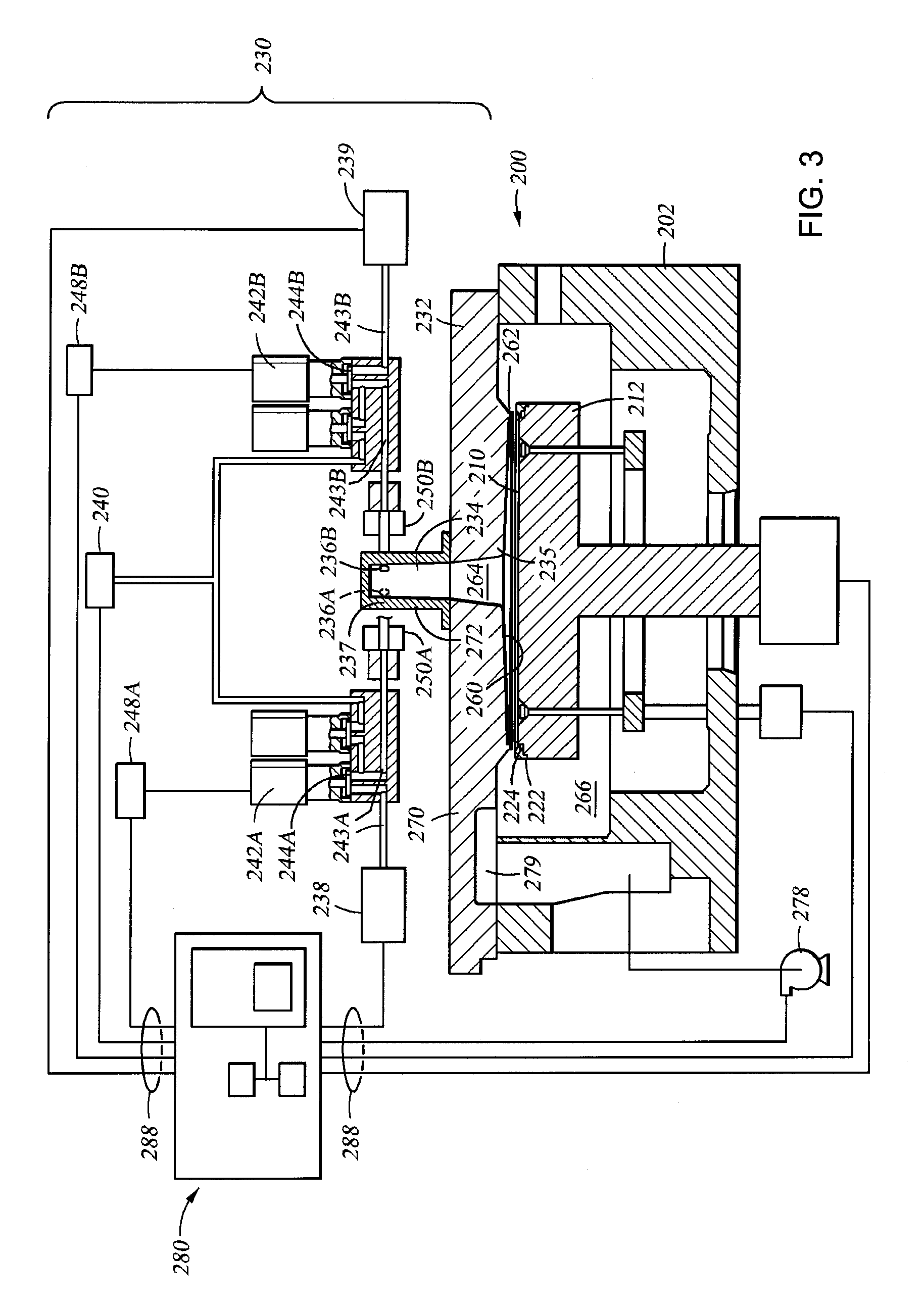
Embodiments of the invention provide methods for forming hafnium materials, such as oxides and nitrides, by sequentially exposing a substrate to hafnium precursors and active oxygen or nitrogen species (e.g., ozone, oxygen radicals, or nitrogen radicals). The deposited hafnium materials have significantly improved uniformity when deposited by these atomic layer deposition (ALD) processes. In one embodiment, an ALD chamber contains an expanding channel having a bottom surface that is sized and shaped to substantially cover a substrate positioned on a substrate pedestal. During an ALD process for forming hafnium materials, process gases form a vortex flow pattern while passing through the expanding channel and sweep across the substrate surface. The substrate is sequentially exposed to chemical precursors that are pulsed into the process chamber having the vortex flow.

Description

CROSS-REFERENCE TO RELATED APPLICATIONS [0001] This application is a continuation of co-pending U.S. Ser. No. 10 / 247,103, filed Sep. 19, 2002, which claims priority from U.S. Ser. No. 60 / 388,929, filed Jun. 14, 2002, which are both incorporated herein by reference in their entirety.BACKGROUND OF THE INVENTION [0002] 1. Field of the Invention [0003] Embodiments of the present invention relate to deposition methods for forming thin films of metal compounds, such as metal oxides or metal nitrides, on substrates for use in manufacturing semiconductor devices, flat-panel display devices, and other electronic devices. [0004] 2. Description of the Related Art [0005] In the field of semiconductor processing, flat-panel display processing or other electronic device processing, chemical vapor deposition (CVD) has played an important role in forming films on substrates. As the geometries of electronic devices continue to shrink and the density of devices continues to increase, the size and asp...

Claims


Application Information

Patent Timeline
Patent Type & Authority Applications(United States)
IPC IPC(8): C23C16/00H01L21/31C23C16/40C23C16/44C23C16/452C23C16/455H01L21/285H01L21/316H01L21/318
CPCC23C16/405C23C16/452C23C16/45542H01L21/318H01L21/28562H01L21/31604C23C16/45553H01L21/02274H01L21/0228H01L21/02181
Inventor METZNER, CRAIG R.KHER, SHREYAS S.GOPAL, VIDYUTHAN, SHIXUEATHREYA, SHANKARRAM A.
Owner APPLIED MATERIALS INC
Learn More