Pulse generating circuit, electronic device using this pulse generating circuit, cellular phone set, personal computer, and information transmitting method using this circuit
a technology of pulse generating circuit and pulse generating circuit, which is applied in the direction of pulse technique, generating/distributing signals, instruments, etc., can solve the problems of increasing power consumption, difficult or impossible to obtain such an element, and heavy use of waveform shown here, so as to facilitate wireless transmission of the required information and reduce power consumption. the effect of significant
- Summary
- Abstract
- Description
- Claims
- Application Information
AI Technical Summary
Benefits of technology
Problems solved by technology
Method used
Image
Examples
first embodiment
[0081]FIG. 1A is a circuit diagram showing a principal portion of a pulse generating circuit according to a first embodiment of the invention, FIGS. 1B to 1D are time charts for describing the operation thereof. However, the description will be made of an example in which the pulse waveform assumes a shape as shown in FIG. 6A and four pulses are contained in a time PD (PD=8Pw) that is, a pulse whose number of fingers is four.
[0082] Reference numerals 101 to 109 shown in FIG. 1A are cascaded inverter circuits. The respective input / output terminals are designated by terminal names such as D-0 to D9.
[0083] When the input terminal D0 is changed from a high level (H) to a low level (L) as shown in FIG. 1B, the respective outputs are propagated with the delay of t. NOT-AND (NAND) circuits 110 to 113 output L from the terminals ND1 to ND4 as shown in FIG. 1C when both D1 and D2, D3 and D4, D5 and D6, and D7 and D0 are H, respectively. The NEITHER-NOR (NOR) circuit (NOR circuit of negativ...
second embodiment
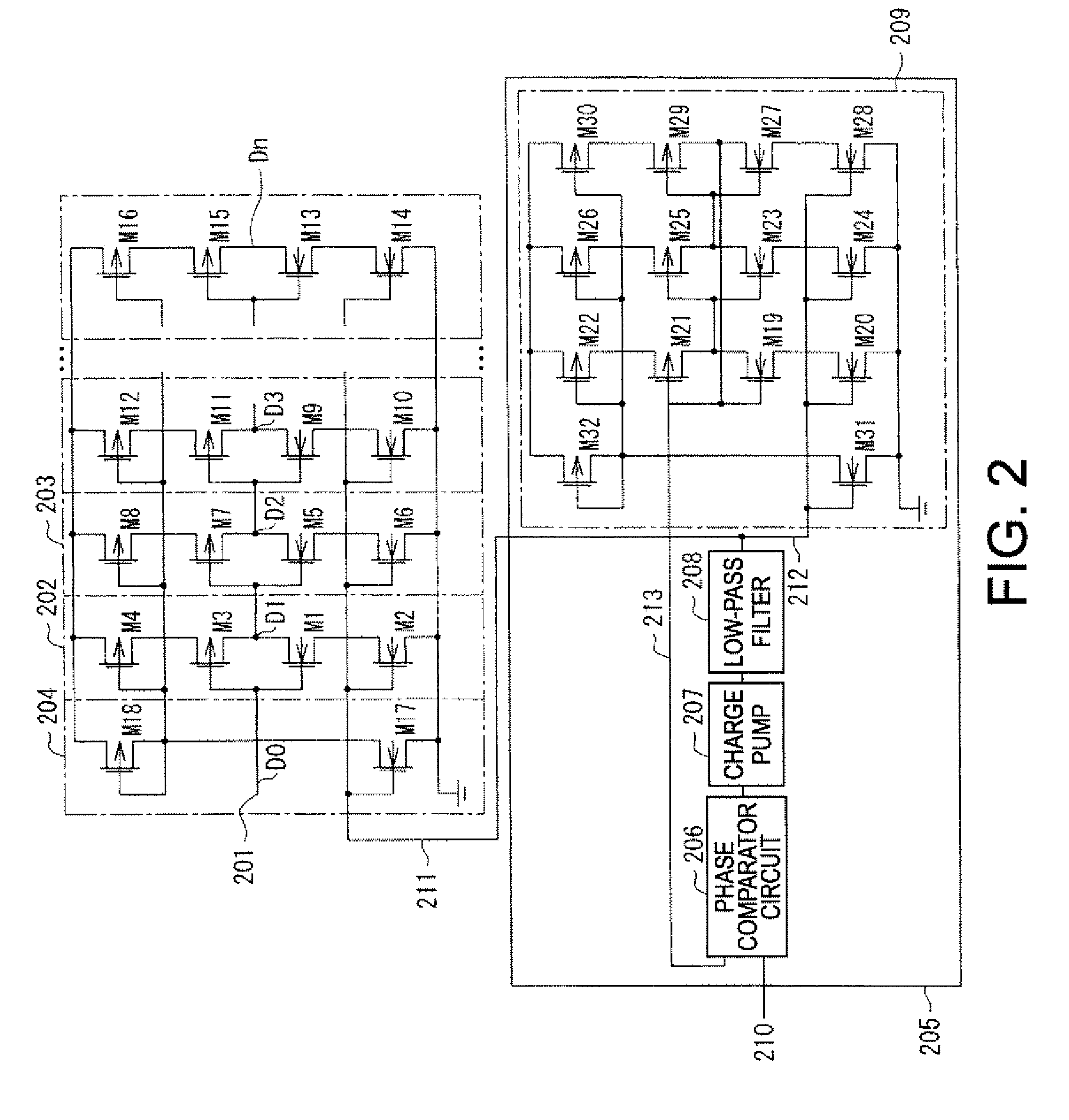
[0089]FIG. 2 is a circuit diagram showing a principal portion of a pulse generating circuit according to a second embodiment of the invention.
[0090] Reference numerals 202, 203 designate inverter circuits in which the amount of delay can be controlled and correspond to the inverter circuits 101, 102 which constitutes the delay circuit in the first embodiment. The equivalent circuits are arranged in the required number of stages for use. In FIG. 2, those from the third stage on are not numbered. The inverter circuit 202 is configured by a combination of a PMOS transistor M3 and an NMOS transistor M1.
[0091] PMOS and NMOS transistors M4 and M2 are connected to sources of the respective transistors M3 and M1, and the amount of delay can be controlled by controlling the amount of electric current flowing into the inverter circuit by the M4 and M2.
[0092] A gate of the transistor M2 is connected to a control voltage terminal 211, and a gate of the transistor M4 is connected to the contr...
third embodiment
[0103]FIG. 3 is a circuit diagram showing a principal portion of a pulse generating circuit according to a third embodiment of the invention.
[0104] Reference numerals 311 to 314 are buffer circuits configured of current mode logic circuits. The contents thereof will be described with the buffer circuit 311 as an example. A differential amplifier circuit is configured by an NMOS transistor differential pair M1 and M2. The NMOS transistor M3 controls the amount of delay by controlling the circuit current according to a control voltage 310 applied to the gate. PMOS transistors M4, M5 are loads on the output side and control the output amplitude by the gate application voltage. Input and output of the buffer circuit 311 is driven by a differential signal which is a characteristic of the current mode logic circuit.
[0105] The terminal 301 is a trigger terminal which corresponds to the terminal D0 in the first embodiment, and intended pulses are generated on the basis of the pulses which...
PUM
 Abstract
Description
Claims
Application Information
 - R&D
- Intellectual Property
- Life Sciences
- Materials
- Tech Scout
- Unparalleled Data Quality
- Higher Quality Content
- 60% Fewer Hallucinations
Browse by: Latest US Patents, China's latest patents, Technical Efficacy Thesaurus, Application Domain, Technology Topic, Popular Technical Reports.
© 2025 PatSnap. All rights reserved.Legal|Privacy policy|Modern Slavery Act Transparency Statement|Sitemap|About US| Contact US: help@patsnap.com


