
Non-intrusive plasma monitoring system for arc detection and prevention for blanket CVD films

a plasma monitoring system and blanket technology, applied in the field of blanket cvd arc detection and prevention, can solve the problems of reducing the yield of working semiconductor devices fabricated on the wafer, reducing the temperature of such cvd processes compared to thermal cvd processes, and the current methods of diagnosing arcing probems in pecvd processing chambers have significant limitations, so as to reduce arcing

Inactive Publication Date: 2007-02-22
APPLIED MATERIALS INC
View PDF14 Cites 37 Cited by
  • Summary
  • Abstract
  • Description
  • Claims
  • Application Information

AI Technical Summary

Benefits of technology

[0010] Embodiments of the invention may further relate to methods to reduce arcing in a semiconductor wafer processing chamber. The methods may include the step of measuring a spike in a DC bias voltage of a process-gas distribution faceplate as a plasma is formed in the processing c...

Problems solved by technology

The high reactivity of the ionized species in the plasma reduces the energy required for a chemical reaction to take place, and thus lowers the temperature for such CVD processes as compared to thermal CVD processes.
This arcing can cause defects in the substrate wafer surface that reduces the yield of working semiconductor devices fabricated on the wafer.
Current methods of diagnosing arcing probems in PECVD processing chambers have significant limitations.
Unfortunately, the S-probe itself can interfere with and destabilize the plasma it is trying to measure.
Contamination and corrosion of the surface of the S-probe can also create a source of particulates which can contaminate the underlying substrate wafer.
While this method avoids placing a probe directly in the plasma, the measurements generally suffer from poor signal-to-noise ratios and poor time resolution that can make it difficult to detect evidence of arcing (e.g., voltage spikes).

Method used


Image

  • Non-intrusive plasma monitoring system for arc detection and prevention for blanket CVD films
  • Non-intrusive plasma monitoring system for arc detection and prevention for blanket CVD films
  • Non-intrusive plasma monitoring system for arc detection and prevention for blanket CVD films

Examples


example substrate processing

System

[0031] One suitable substrate processing system in which the method of the present invention can be carried out is shown in FIGS. 3A and 3B, which are vertical, cross-sectional views of a CVD system 10, having a vacuum or processing chamber 15 that includes a chamber wall 15a and a chamber lid assembly 15b. The chamber wall 15a and chamber lid assembly 15b are shown in exploded, perspective views in FIGS. 3C and 3D.

[0032] The CVD system 10 contains a gas distribution fold 11 for dispersing process gases to a substrate (not shown) that rests on a heated pedestal 12 centered within the process chamber 15. During processing, the substrate (e.g., a semiconductor wafer) is positioned on a flat (or slightly convex) surface 12a of the pedestal 12. The pedestal 12 can be moved controllably between a lower loading / off-loading position (depicted in FIG. 3A) and an upper processing position (indicated by dashed line 14 in FIG. 3A and shown in FIG. 3B), which is closely adjacent to the m...

example 1

Arcing During Deposition of FSG Film

[0047] In these examples, fluorine-doped-silicate (FSG) layers (generally having a 8 μm thickness) were deposited on a 300 mm silicon-on-insulator (SOI) substrate wafers in PECVD processes. The PECVD processing chamber used for the depositions was a Producer™ SE chamber made by Applied Materials, Inc. of Santa Clara, Calif. Plasma was generated and deposited on the substrate wafers using a dual-frequency RF power source that supplied high-frequency (i.e., 13.56 MHz) RF power and low-frequency (i.e., 350 kHz) RF power to the processing chamber. Table 1 shows additional processing details for various phases of a standard deposition run in the chamber:

TABLE 1Baseline FSG Layer Deposition Run with PECVD Producer ChamberProcessTOESInitiationDepositionTerminationExhaustConditionOnPhasePhasePhasePhaseMax Time101-282210(sec)Temp (° C.)400400400400400Pressure (Torr)66660Heater Space285285285285285(mils)RF Time (sec)018220HF RF Power01250160016000(Watts...

example 2

Arcing During Deposition of Integrated USG-FGS Film

[0053] In this example, an integrated undoped silicate glass (USG) and fluorine-doped-silicate (FSG) film was deposited on a 300 mm silicon-on-insulator (SOI) substrate wafer in a PECVD process. The PECVD processing chamber used for the deposition was a Producer™ SE chamber made by Applied Materials, Inc. of Santa Clara, Calif. Plasma was generated and deposited on the substrate wafer using a dual-frequency RF power source that supplied high-frequency (i.e., 13.56 MHz) RF power and low-frequency (i.e., 350 kHz) RF power to the processing chamber. The deposition started with the depositing of the USG material on the substrate wafer, followed by a transition to the deposition of the FSG material.

[0054] In a baseline process example, the transition from USG to FSG depositions was discontinuous with the USG process gases and RF power being terminated before the FSG process gases and RF power is initiated. FIG. 6 shows a plot of the D...


PUM

PropertyMeasurementUnit
Fractionaaaaaaaaaa
Frequencyaaaaaaaaaa
Poweraaaaaaaaaa

Abstract

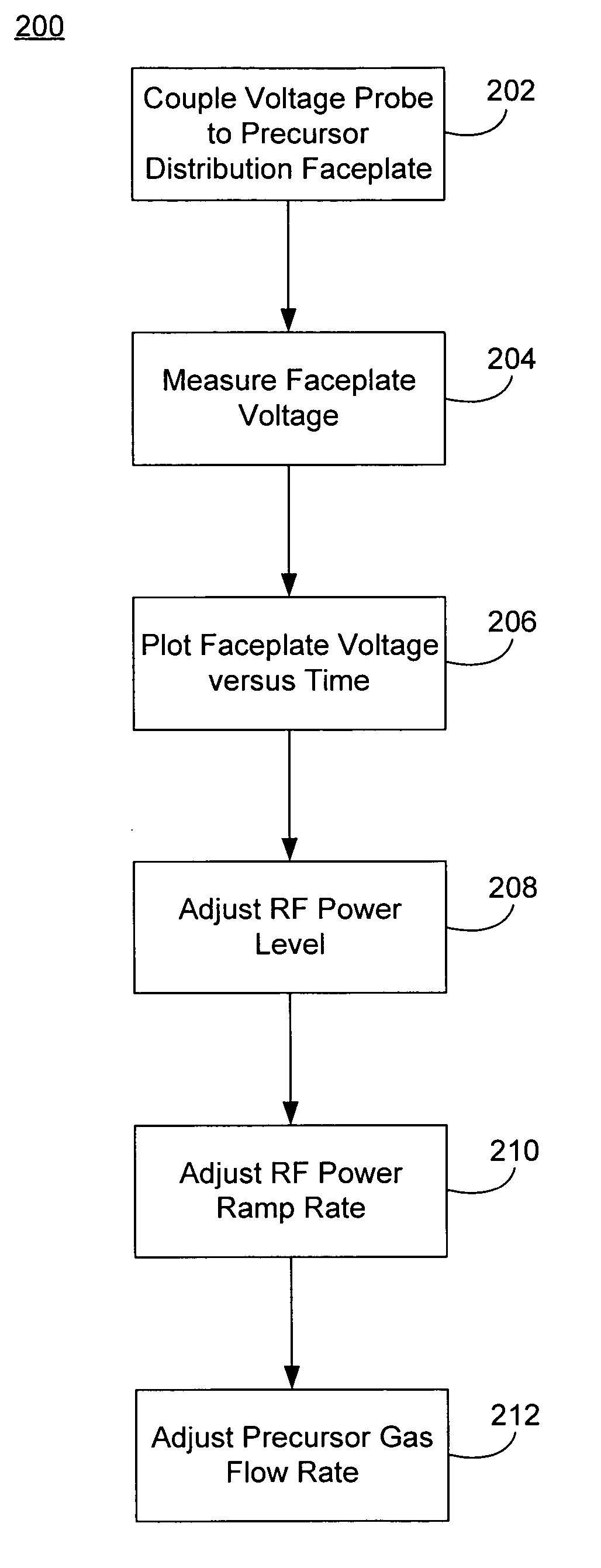
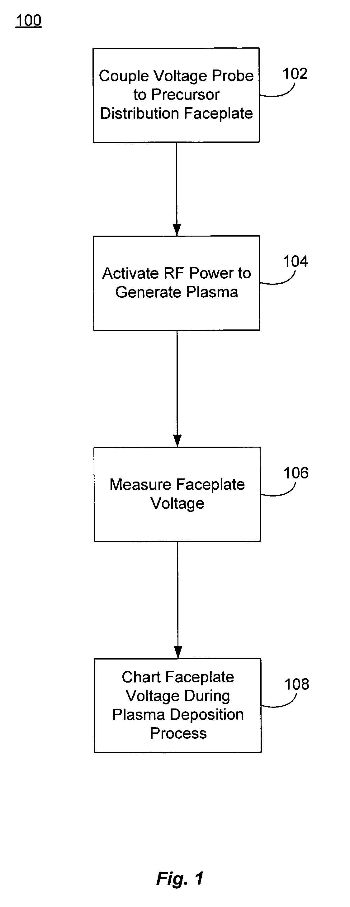
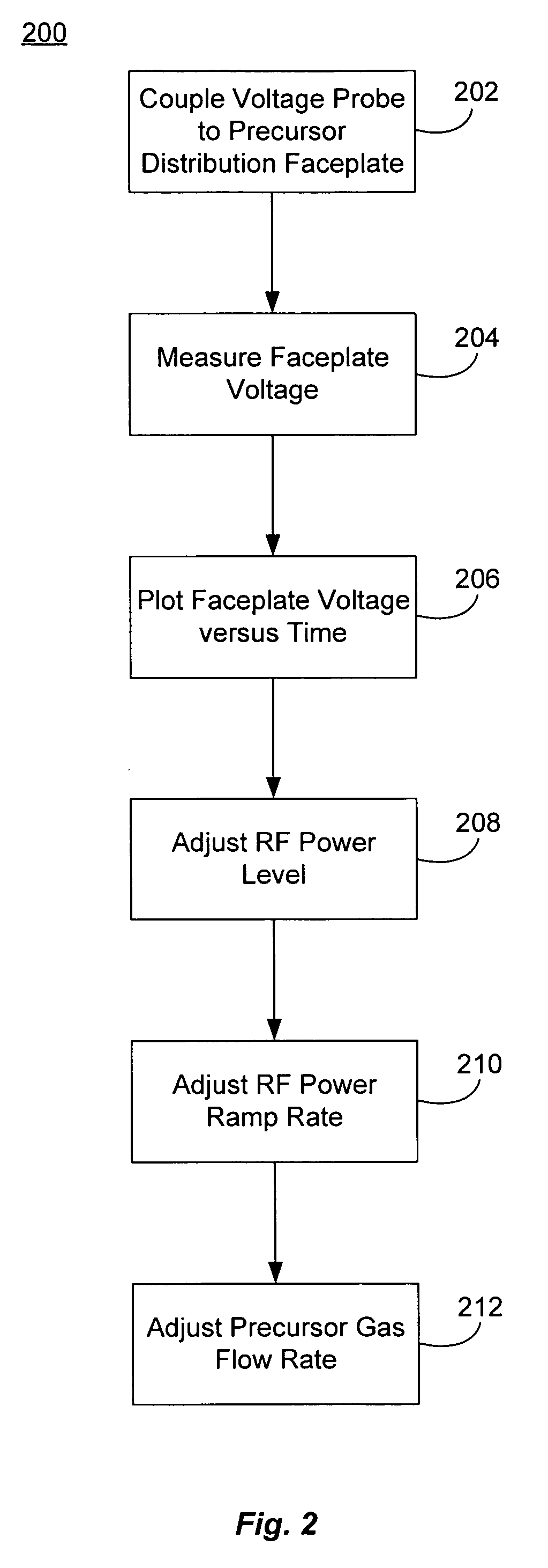
Methods and systems of diagnosing an arcing problem in a semiconductor wafer processing chamber are described. The methods may include coupling a voltage probe to a process-gas distribution faceplate in the processing chamber, and activating an RF power source to generate a plasma between the faceplate and a substrate wafer. The methods may also include measuring the DC bias voltage of the faceplate as a function of time during the activation of the RF power source, where a spike in the measured voltage at the faceplate indicates an arcing event has occurred in the processing chamber. Methods and systems to reduce arcing in a semiconductor wafer processing chamber are also described.

Description

CROSS-REFERENCES TO RELATED APPLICATIONS [0001] NOT APPLICABLE BACKGROUND OF THE INVENTION [0002] The fabrication of modern semiconductor devices commonly involve the formation of thin films on a semiconductor wafer substrate though the chemical reaction of gases. Such deposition processes are referred to a chemical vapor deposition (CVD). Conventional thermal CVD processes supply reactive gases to the substrate surface where heat-induced chemical reactions take place to produce a desired film. [0003] An alternative method of depositing layers over a substrate includes plasma enhanced CVD (PECVD) techniques. Plasma enhanced CVD techniques promote excitation and / or dissociation of the reactant gases by the application of radio frequency (RF) energy to a reaction zone near the substrate surface, thereby creating a plasma. The high reactivity of the ionized species in the plasma reduces the energy required for a chemical reaction to take place, and thus lowers the temperature for such ...

Claims


Application Information

Patent Timeline
IPC IPC(8): H05H1/24B05C11/00C23C16/00
CPCH01J37/32935H01J2237/24592H01J37/32944
Inventor SOO, JYR HONGNGUYEN, VU NGOC TRANREITER, STEVENFOSTER, JASONKIM, BOK HOENM'SAAD, HICHEM
Owner APPLIED MATERIALS INC
Learn More