Liquid crystal display device repair system and method thereof
a liquid crystal display and repair system technology, applied in static indicating devices, non-linear optics, instruments, etc., can solve the problems of inefficient power consumption and decrease the yield of acceptable devices
- Summary
- Abstract
- Description
- Claims
- Application Information
AI Technical Summary
Problems solved by technology
Method used
Image
Examples
first embodiment
[0021] The repair process of the LCD device will now be described with reference to FIG. 3. As shown, if an open occurs at an i-th (where i is a natural number) data line DLi, the laser repair process will short the i-th data line DLi to the adjacent first repair line 112 at intersection 116a. Further, the laser repair process will short the i-th data line DLi and the adjacent second repair line 114 at intersection 116b. Thereafter, the power voltage terminal Vcc and the repair amplification terminal RA of the operational amplifier 128 of the data driver IC 104 connected to the i-th data line DLi are opened by a laser cutting process. This allows the pixel voltage signal on the i-th data line DLi to be supplied to the input terminal IT of the operational amplifier 128 through the first repair line 112. Then the operational amplifier 128 generates a repair pixel voltage signal by amplifying the pixel voltage signal. The repair pixel voltage signal is supplied to the i-th data line DL...
second embodiment
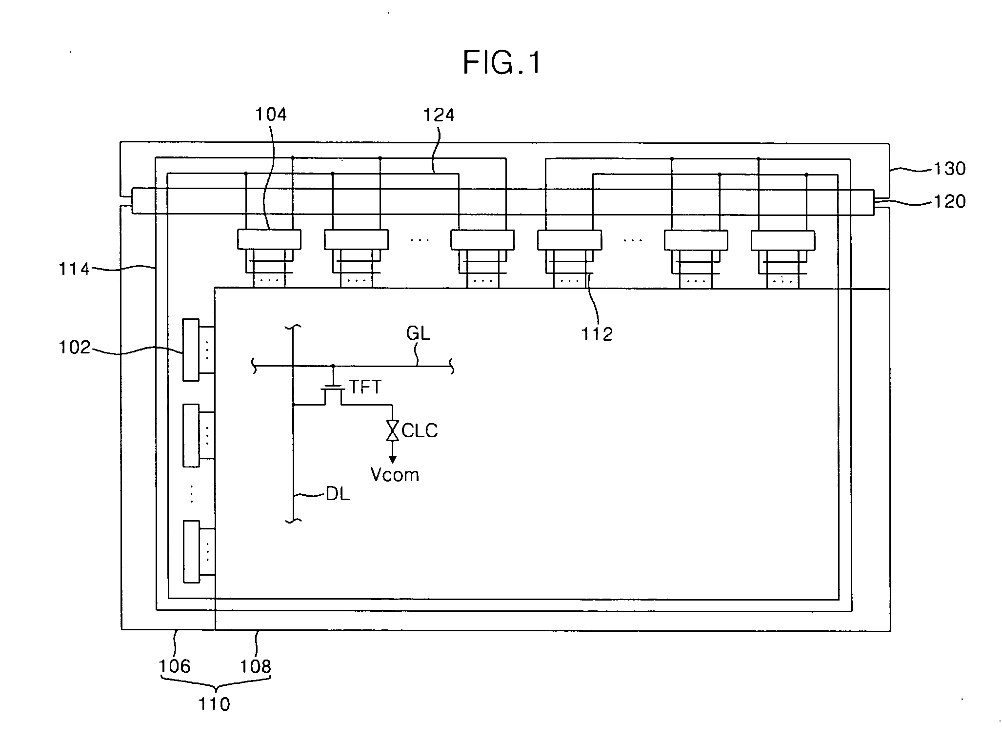
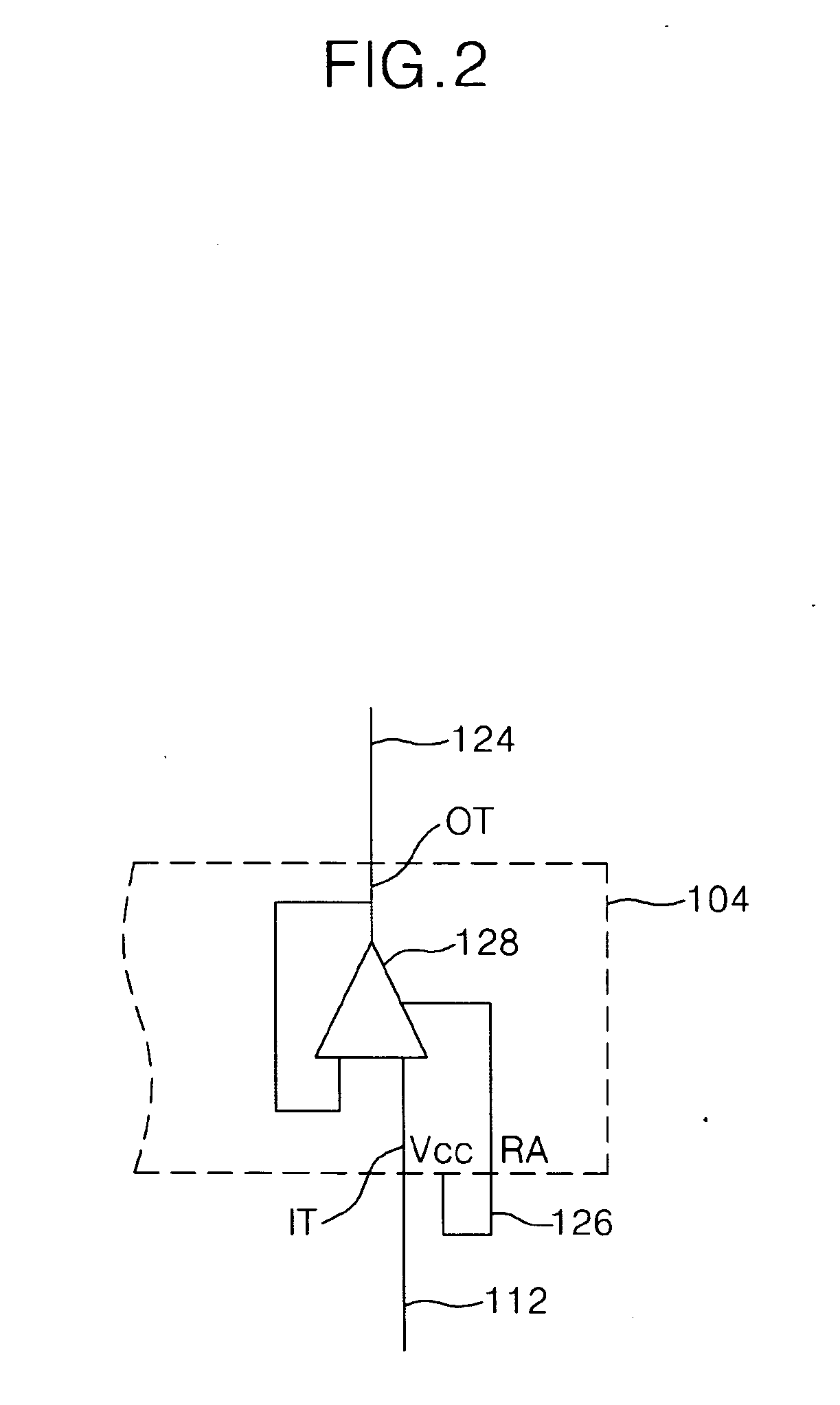
[0024]FIG. 4 illustrates an LCD device according to the present invention. The LCD device of FIG. 4 includes the same elements as the LCD device of FIG. 1 except that input terminals of operational amplifiers 128 are commonly connected to the first passing line 122 formed on the FPC 120 and the PC 130. Therefore, a detailed description of the same elements will be omitted. The operational amplifier 128 prevents a delay of a repair pixel voltage signal caused by the second repair line 114 formed to detour the display region. For this, the operational amplifier 128 includes the input terminal IT connected to the first passing line 122 through the first repair line 112, the output terminal OT connected to the second repair line 114 through a second passing line 124, and the power voltage terminal Vcc and repair amplification terminal RA which are commonly connected to the common line 126 formed in a ‘U’ shape on the lower substrate.
[0025] When the power voltage terminal Vcc and repair ...
third embodiment
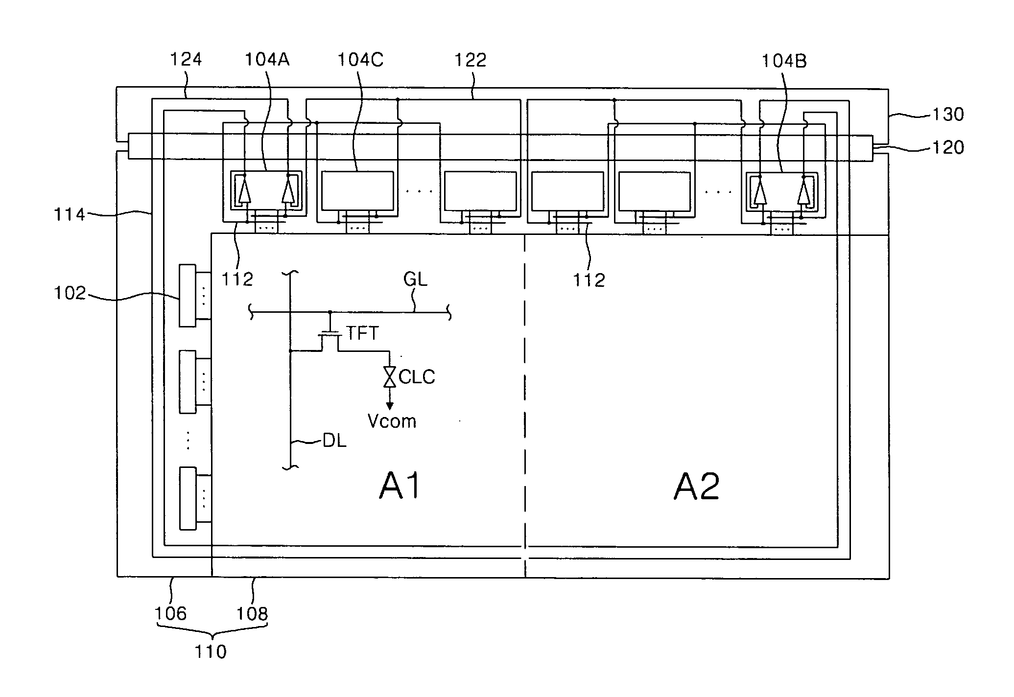
[0044]FIG. 7 illustrates an LCD device according to the present invention. The LCD device of FIG. 7 includes the same elements as that of FIG. 4 except that the passing line is formed on the thin film transistor substrate 106. Therefore, a detailed description of the same elements will not be given. The operational amplifiers 128 included in the data driver ICs 104 maintain a disabled state if no opened data line is detected. However, if an opened data line is detected, the operational amplifiers included in the first and last data driver ICs 104A and 104B become an enabled state, and the operational amplifiers included in the other data driver ICs 104C except the first and last data driver ICs 104A and 104B maintain a disabled state.
[0045] Input terminals of the operational amplifiers included in the respective data driver ICs 104 are commonly connected to the passing lines 122 through the first repair line 112. Since the passing lines 122 are formed on the thin film transistor sub...
PUM
 Abstract
Description
Claims
Application Information
 - R&D
- Intellectual Property
- Life Sciences
- Materials
- Tech Scout
- Unparalleled Data Quality
- Higher Quality Content
- 60% Fewer Hallucinations
Browse by: Latest US Patents, China's latest patents, Technical Efficacy Thesaurus, Application Domain, Technology Topic, Popular Technical Reports.
© 2025 PatSnap. All rights reserved.Legal|Privacy policy|Modern Slavery Act Transparency Statement|Sitemap|About US| Contact US: help@patsnap.com


