
Method for preventing charge-up in plasma process and semiconductor wafer manufactured using same

a plasma process and semiconductor technology, applied in semiconductor devices, solid-state devices, decorative arts, etc., can solve the problems of arcing of accumulated electric charge and charge-up phenomenon, and achieve the effects of preventing charge-up, and reducing electric charge accumulation

Inactive Publication Date: 2007-02-22
SAMSUNG ELECTRONICS CO LTD
View PDF2 Cites 10 Cited by
  • Summary
  • Abstract
  • Description
  • Claims
  • Application Information

AI Technical Summary

Benefits of technology

[0010] According to some embodiments, a method of preventing charge-up in a plasma process is capable of reducing accumulation of electric charge on the surface of a semiconductor wafer during a plasma etching process.
[0011] According to some embodiments, a semiconductor wafer is capable of reducing accumulation of electric charge on its surface during a plasma etching process.

Problems solved by technology

However, reaction products that include a large amount of electric charge may accumulate on the surface of the exposed wafer in plasma etching.
While, such reaction products may be removed to some degree through the exhausting process, etc., most electric charges are trapped and accumulate near a conductive pattern, thereby causing a charge-up phenomenon.
This leads to arcing of the accumulated electric charge due to stress between the narrow conductive patterns.

Method used


Image

  • Method for preventing charge-up in plasma process and semiconductor wafer manufactured using same
  • Method for preventing charge-up in plasma process and semiconductor wafer manufactured using same
  • Method for preventing charge-up in plasma process and semiconductor wafer manufactured using same

Examples


Embodiment Construction

[0017] The invention will now be described more fully hereinafter with reference to the accompanying drawings, in which exemplary embodiments of the invention are shown.

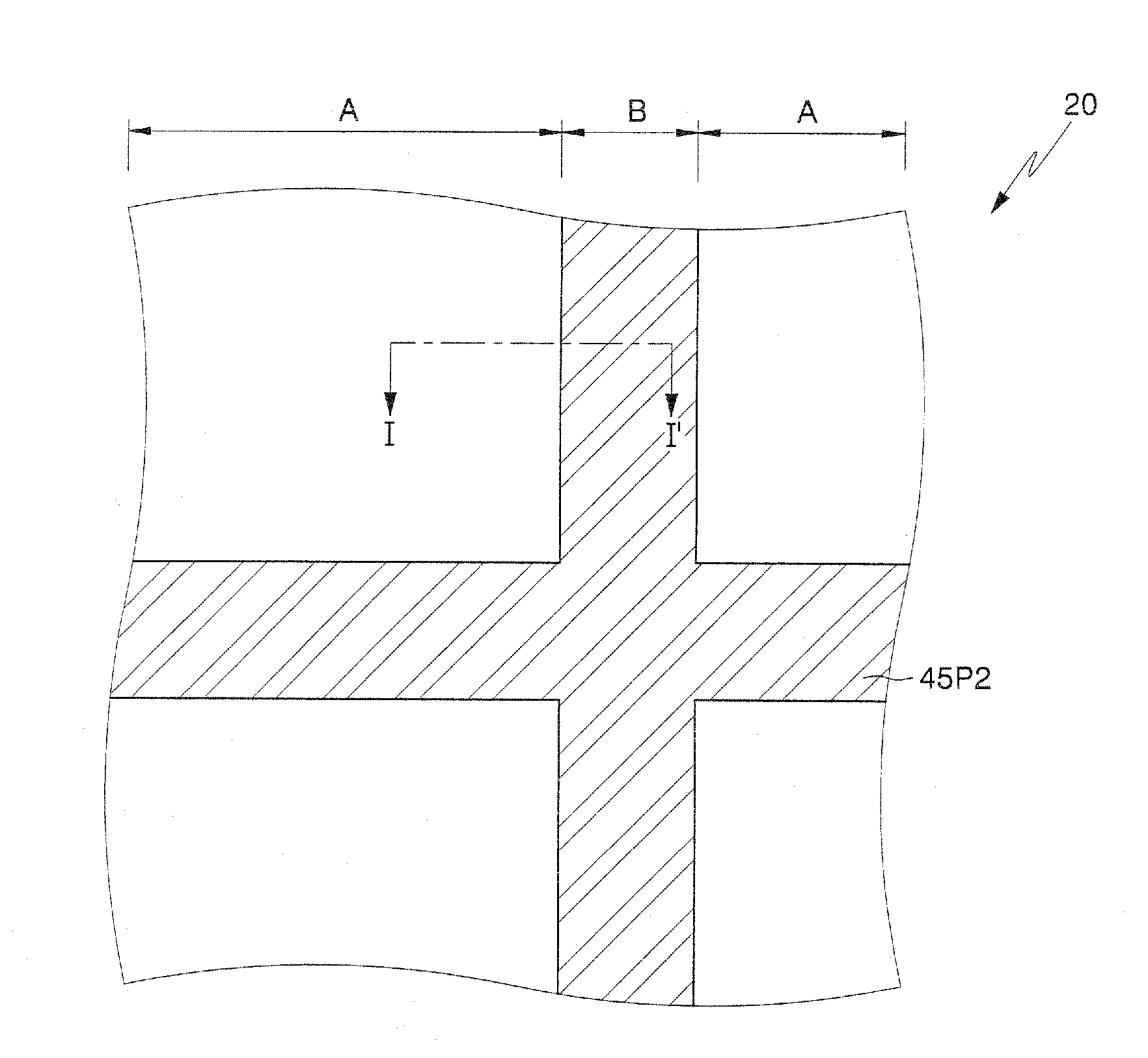
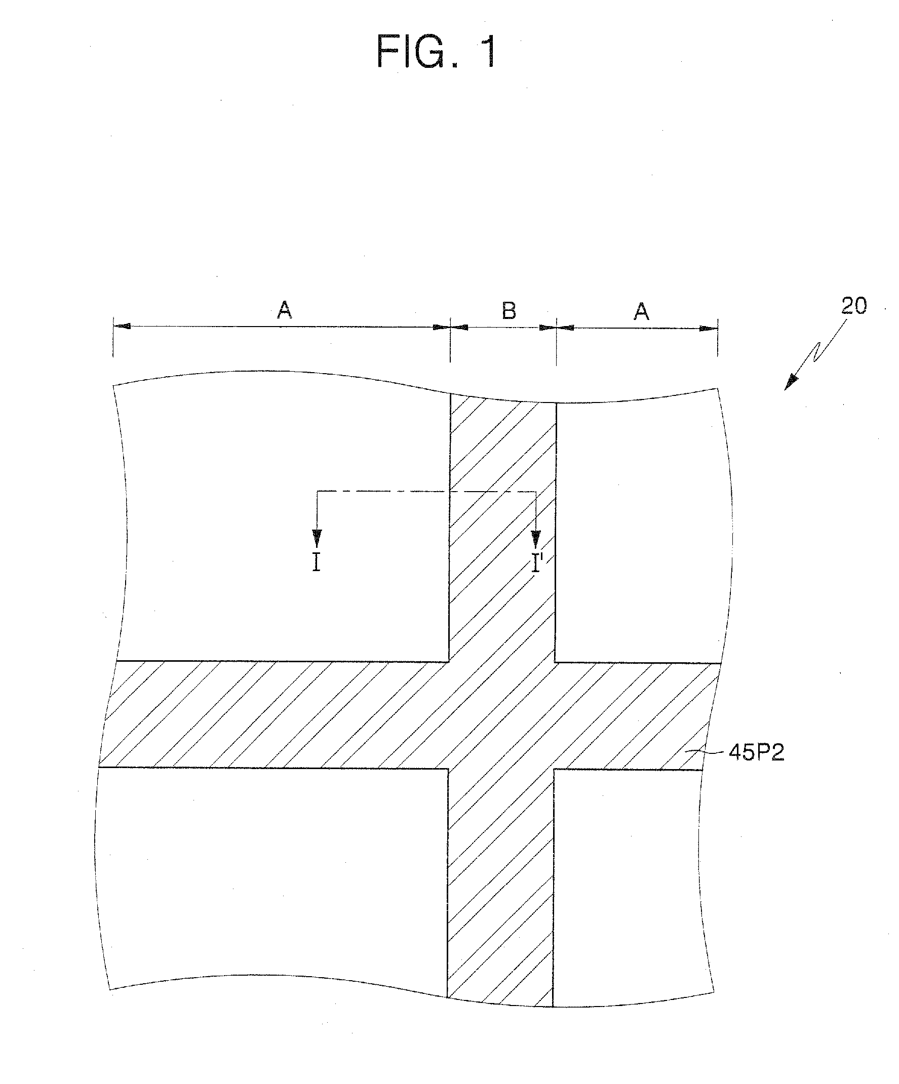
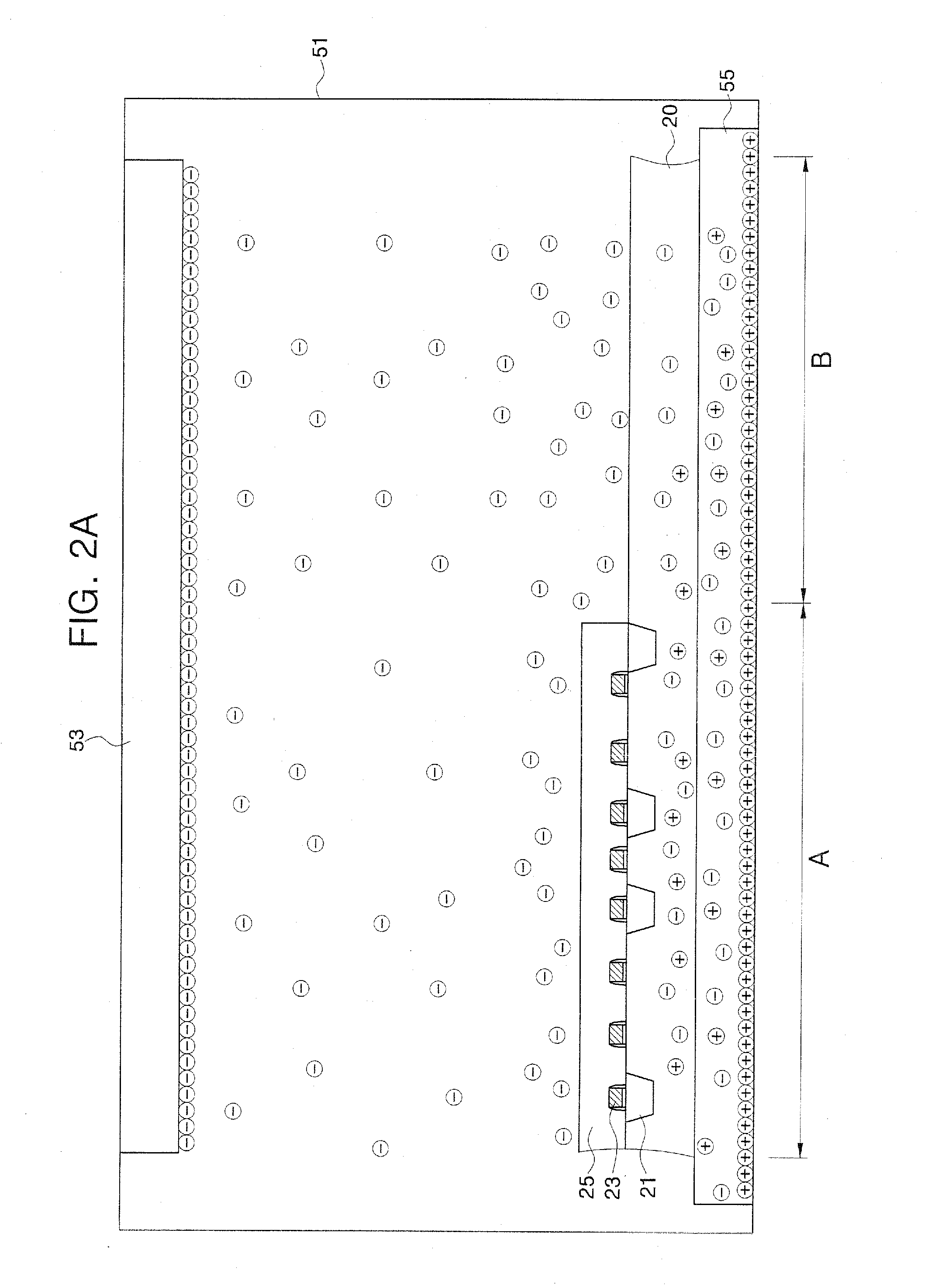
[0018]FIG. 1 is a plan diagram that illustrates part of a semiconductor wafer in accordance with some embodiments of the invention. FIGS. 2A through 2M are cross-sectional diagrams, taken along line I-I′ of FIG. 1, which illustrate exemplary processes in a method for preventing charge-up in a plasma process in accordance with some embodiments of the invention.

[0019] As shown in FIG. 1, semiconductor chip regions A and scribe line regions B adjacent to the semiconductor chip regions are defined on a semiconductor wafer 20. The semiconductor wafer 20 has an interlayer insulating layer (not illustrated) that covers the semiconductor chip regions A and exposes the scribe line regions B. A conductive pattern (not illustrated) is disposed to contact a part of the semiconductor chip regions A through the interlayer insula...


PUM

PropertyMeasurementUnit
electric chargeaaaaaaaaaa
conductiveaaaaaaaaaa
semiconductoraaaaaaaaaa

Abstract

A method for preventing plasma charge-up of a semiconductor wafer includes defining a semiconductor chip region and a scribe line region on a semiconductor wafer, forming an interlayer insulating layer pattern on the wafer, the interlayer insulating layer pattern exposing the scribe line region, plasma etching the interlayer insulating layer pattern to form a contact hole that exposes the semiconductor chip region, and during the plasma etching, discharging an electric charge generated by the plasma etching through the scribe line region.

Description

CROSS-REFERENCE TO RELATED APPLICATIONS [0001] This application claims priority from Korean Patent Application No. 10-2005-75439, which was filed on 17 Aug. 2005. Korean Patent Application No. 10-2005-75439 is incorporated by reference in its entirety. BACKGROUND [0002] 1. Technical Field [0003] This disclosure relates to a method for preventing charge-up in a plasma process and a semiconductor wafer manufactured thereby, and more particularly, to a method for preventing charge-up in a plasma process by which electric charge generated during a plasma process is discharged through a scribe line region, and a semiconductor wafer manufactured thereby. [0004] 2. Discussion of the Related Art [0005] A semiconductor device manufacturing process typically includes deposition of a thin film or layer on the surface of a semiconductor wafer. Another layer may be formed between the semiconductor wafer and the thin film. One method to carry out the deposition of the thin film or layer is using ...

Claims


Application Information

Patent Timeline
Patent Type & Authority Applications(United States)
IPC IPC(8): C23F1/00H01L29/00H01L21/302
CPCC23F4/00H01L27/10894H01L21/32136H01L21/31116H10B12/09H01L21/3065
Inventor KIM, YONG-SAM
Owner SAMSUNG ELECTRONICS CO LTD
Learn More