
Resist composition, method of forming resist pattern, semiconductor device and method of manufacturing thereof

a technology of resist composition and resist pattern, which is applied in the field of resist composition, can solve the problems of poor film forming ability, high crystallinity of nanoedges, and occurrence of nanoedge roughness, and achieve high-quality, high-performance semiconductor devices. high-performance, high-quality results

Inactive Publication Date: 2007-01-04
FUJITSU LTD
View PDF8 Cites 11 Cited by
  • Summary
  • Abstract
  • Description
  • Claims
  • Application Information

AI Technical Summary

Benefits of technology

[0016] Further, although each of the tannin and the derivative thereof is low-molecular substance, the film forming ability thereof is good. Therefore, they can be suitably used in the formation of fine and highly-detailed resist patterns. Moreover, because each of the tannin and derivative thereof is water soluble, water can be used as the coating solvent and the developing liquid, and costs and the burden on the environment are reduced. In particular, in a case in which the tannin is a natural product, the burden on the environment is reduced even more.
[0017] The method of forming a resist pattern according to the present invention comprises: forming a resist film on a surface of an object to be processed, by using a resist composition; and exposing and developing the resist film, wherein the resist composition contains at least one of a tannin and a derivative thereof. In this method of forming a resist pattern, after a resist film is formed, by using the resist composition according to the present invention, on the surface of an object to be processed, the resist film is exposed and developed. As a result, a resist pattern can be formed simply, efficiently, and at a low cost. Because the resist pattern is formed by using the resist composition according to the present invention which contains at least one of a tanin and a derivative thereof, the resist pattern is fine and highly-detailed, and does not have nanoedge roughness which can cause problems.
[0019] In this method of manufacturing a semiconductor device, first, the resist film is formed by using the resist composition according to the present invention on the surface of an object on which a pattern such as a wiring pattern is formed thereafter, and then the resist film is exposed and developed. Thus, a fine and highly-detailed resist pattern can be formed without nanoedge roughness which can cause problems. Next, by performing an etching using the resist pattern thus formed as a mask, the surface of the object is patterned finely and in great detail and with good dimensional accuracy. Therefore, it is possible to efficiently manufacture a high-quality, high-performance semiconductor device, which has a pattern such as a wiring pattern or the like which is extremely fine and is highly detailed and has excellent dimensional accuracy.
[0020] The semiconductor device according to the present invention is manufactured by the method of manufacturing a semiconductor device according to the present invention. This semiconductor device has a pattern such as a wiring pattern or the like which is extremely fine and is highly detailed and has excellent dimensional accuracy, and the semiconductor device is high-quality and high-performance.

Problems solved by technology

As patterns have become more and more fine in recent years, the occurrence of nanoedge roughness has become a great problem.
However, these molecular resists are a special molecular configuration and are expensive (one gram costs from several thousand yen to several ten-thousand yen), and as compared with polymers, the crystallinity thereof is high, and therefore, the film forming ability thereof is poor.
Therefore, the problems arise that the costs and the burden on the environment increase.
Further, although the aforementioned JP-A Nos. 2002-47375 and 2002-53699 mention lignin (a component of wood), there is no disclosure whatsoever of how to use tannins.
Therefore, there is the problem that they cannot aim to reduce nanoedge roughness, reduce costs, and reduce the burden on the environment.
Accordingly, the current situation is that there has not yet been provided a resist composition which can easily and efficiently and at a low cost form a fine, highly-detailed resist pattern at which nanoedge roughness can be suppressed, nor related techniques utilizing such a resist composition.

Method used


Image

  • Resist composition, method of forming resist pattern, semiconductor device and method of manufacturing thereof
  • Resist composition, method of forming resist pattern, semiconductor device and method of manufacturing thereof
  • Resist composition, method of forming resist pattern, semiconductor device and method of manufacturing thereof

Examples


example 1

—Preparation of Resist Composition—

[0111] A resist composition (coating liquid) was prepared on the basis of the following composition.

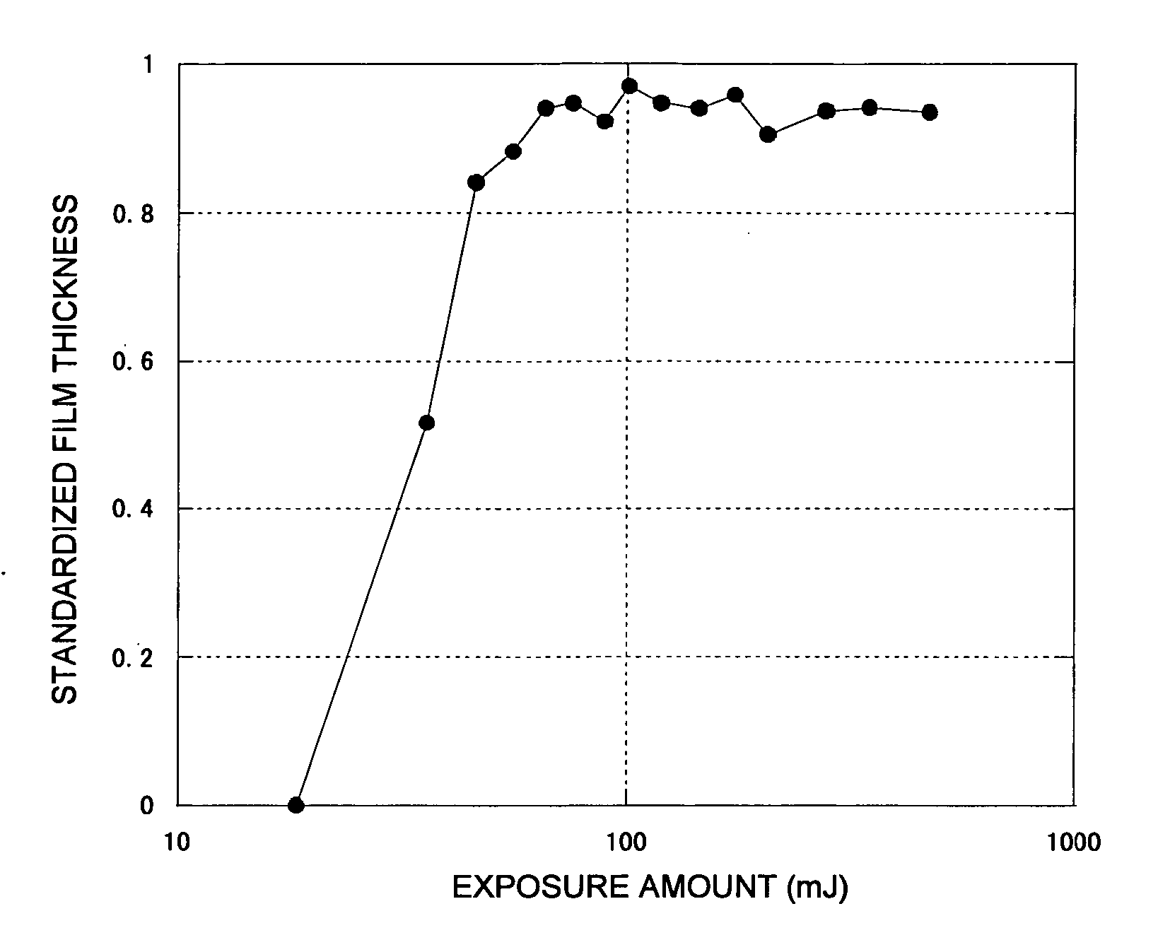
Chinese tannin (hydrolyzable tannin, manufactured by Kanto100parts by massChemical Co., Inc.)Uryl derivative expressed by following structural formula (9) (the20parts by masscrosslinking agent, manufactured by Sanwa Chemical Co., Ltd.)Triphenylsulfonium perfluorobutane sulfonate (acid generator,3parts by massmanufactured by Midori Kagaku Co., Ltd.)Ethyl lactate (solvent, manufactured by Kanto Chemical Co., Inc.)1,000parts by massStructural formula (9)

[0112] When the obtained resist composition was dissolved into THF (tetrahydrofuran) as a solvent and analyzed by gel permeation chromatography, no high molecular mass component corresponding to the polymer was detected.

—Experiment Evaluating Characteristics of Resist Composition—

[0113] The obtained resist composition (coating liquid) was coated to a thickness of 0.3 μm on a silicon wafer and prebakin...

example 2

[0116] Resist compositions were prepared, and experiments evaluating the characteristics of the obtained resist compositions were carried out in the same manner as in Example 1, except that the uryl derivative used as the crosslinking agent in Example 1 was replaced with the urea derivative expressed by following structural formula (8), the pyrogallol derivative expressed by following structural formula (38), and the melamine derivative expressed by following structural formula (7), respectively.

[0117] Note that the pyrogallol derivative expressed by above structural formula (38) is 2,6-bisdroxymethyl-p-cresol.

[0118] When the obtained resist compositions were dissolved into THF (tetrahydrofuran) as a solvent, respectively, and analyzed by gel permeation chromatography, no high molecular mass component corresponding to the polymer was detected.

[0119] The sensitivity curves of the exposure samples prepared by the same method as in Example 1 are shown in FIG. 3 for the urea deriva...

example 3

[0121] A resist composition was prepared, and an experiment evaluating the characteristics of the obtained resist composition was carried out in the same manner as in Example 1, except that the uryl derivative used as the crosslinking agent in Example 1 was replaced with 1-adamantanol (manufactured by Kanto Chemical Co., Inc.) which imparted a polarity change.

[0122] When the obtained resist composition was dissolved in to THF (tetrahydrofuran) as a solvent and analyzed by gel permeation chromatography, no high molecular mass component corresponding to the polymer was detected.

[0123] The sensitivity curve of the exposure sample prepared by the same method as in Example 1 is shown in FIG. 5. From FIG. 5, it can be understood that the resist composition of the present invention using 1-adamantanol behaved as a negative resist. Note that, with 1-adamantanol, an increase in the molecular mass due to the crosslinking reaction does not occur, and therefore, it is clear that the resist be...


PUM

PropertyMeasurementUnit
pressureaaaaaaaaaa
wavelengthaaaaaaaaaa
temperatureaaaaaaaaaa

Abstract

The resist composition of the present invention contains at least one of a tannin and a derivative thereof. The method of forming a resist pattern of the present invention includes: forming a resist film on a surface of an object to be processed, by using the resist composition; and exposing and developing the resist film. The method of manufacturing a semiconductor device of the present invention includes: forming a resist film on a surface of an object to be processed, by using the resist composition; exposing and developing the resist film to form a resist pattern; and patterning the surface of the object by performing an etching through the resist pattern as a mask.

Description

CROSS-REFERENCE TO RELATED APPLICATIONS [0001] This application is based upon and claims the benefit of priority from the prior Japanese Patent Application No. 2005-177031, filed on Jun. 16, 2005, the entire contents of which are incorporated herein by reference. BACKGROUND OF THE INVENTION [0002] 1. Field of the Invention [0003] The present invention relates to a resist composition suited to the formation of a fine, highly-detailed resist pattern, and in particular, to a resist composition using a molecular resist in which the occurrence of nanoedge roughness can be suppressed, and to a method of forming a resist pattern, a semiconductor device, and a method of manufacturing thereof using the resist composition. [0004] 2. Description of the Related Art [0005] Conventionally, polymers are generally used as resist compositions for forming resist patterns, from the standpoint that a coated film can be easily obtained at the time of coating by using the resist composition as a coating ...

Claims


Application Information

Patent Timeline
Patent Type & Authority Applications(United States)
IPC IPC(8): G03C1/00
CPCG03F7/038G03F7/0045
Inventor NAMIKI, TAKAHISANOZAKI, KOJIKOZAWA, MIWA
Owner FUJITSU LTD
Learn More