


Quick Research
Generate reliable direction feasibility study reports for your R&D in just a few steps.

Technical Q&A
Discover and master advanced knowledge NOW. Basics, ideas, possibilities, all at once.

Find Solutions
As an expert in R&D theories, this can generate solutions to your technical problems instantly.

Evaluate Feasibility
Analyze your overall solution with one click, know your potential R&D risks in advance.

Monitor Landscape
Get weekly tech updates, stay abreast of the latest tech innovations and key insights.
SOI bipolar transistors with reduced self heating
a bipolar transistor and self heating technology, applied in the field of bipolar transistors, can solve the problems of reduced collector-base capacitance, high early voltage, and high breakdown voltag
- Summary
- Abstract
- Description
- Claims
- Application Information
AI Technical Summary
Problems solved by technology
Method used
Image

Examples
second embodiment
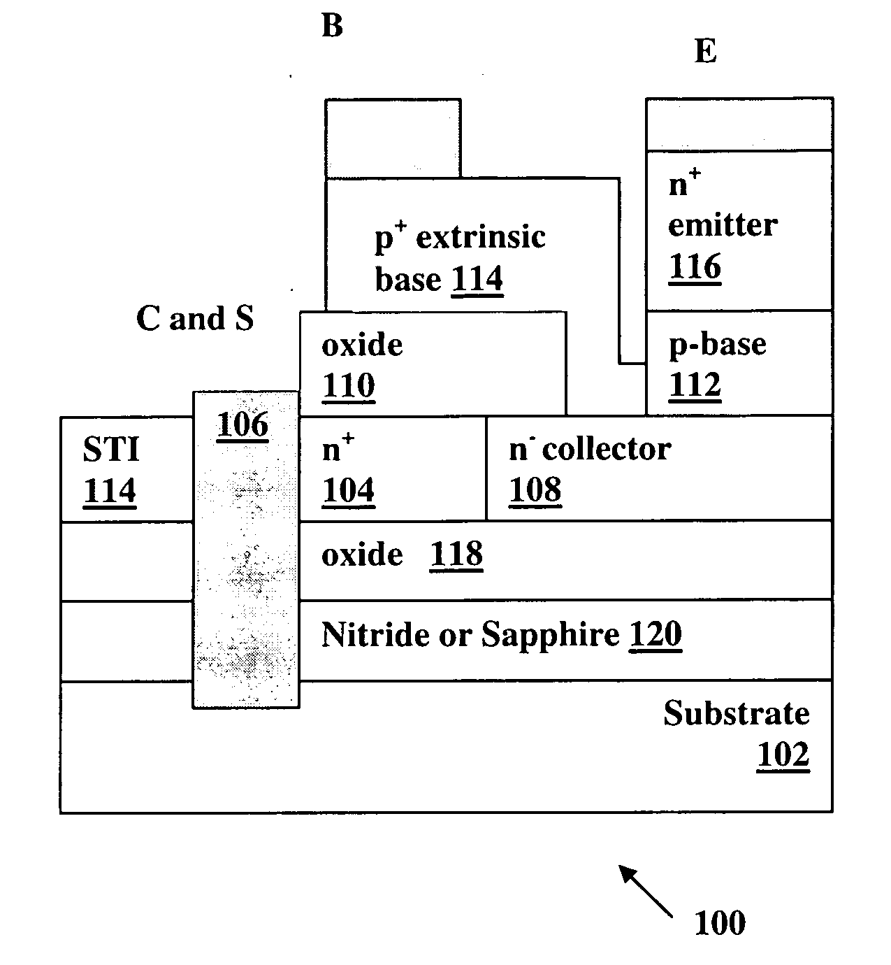
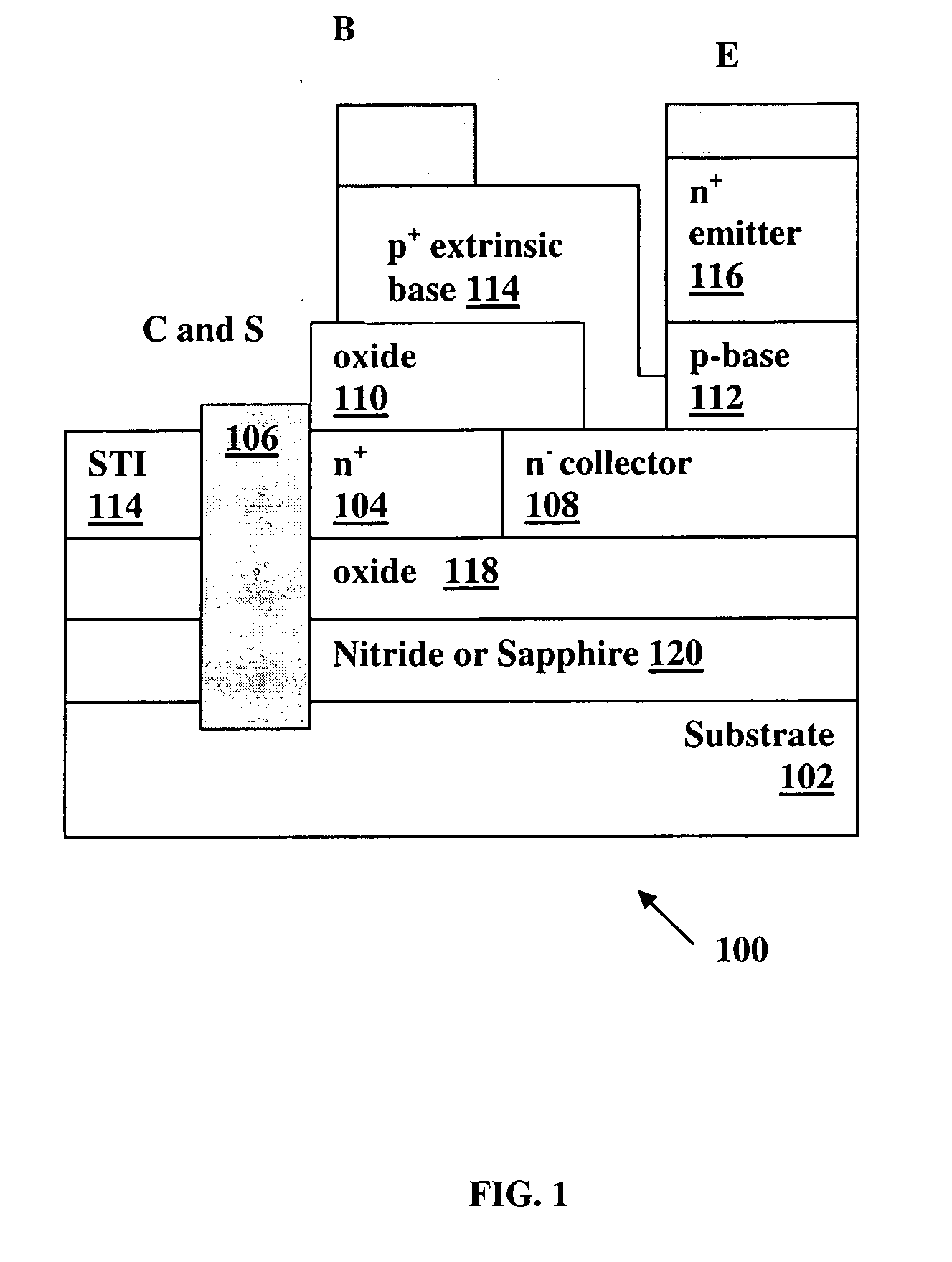
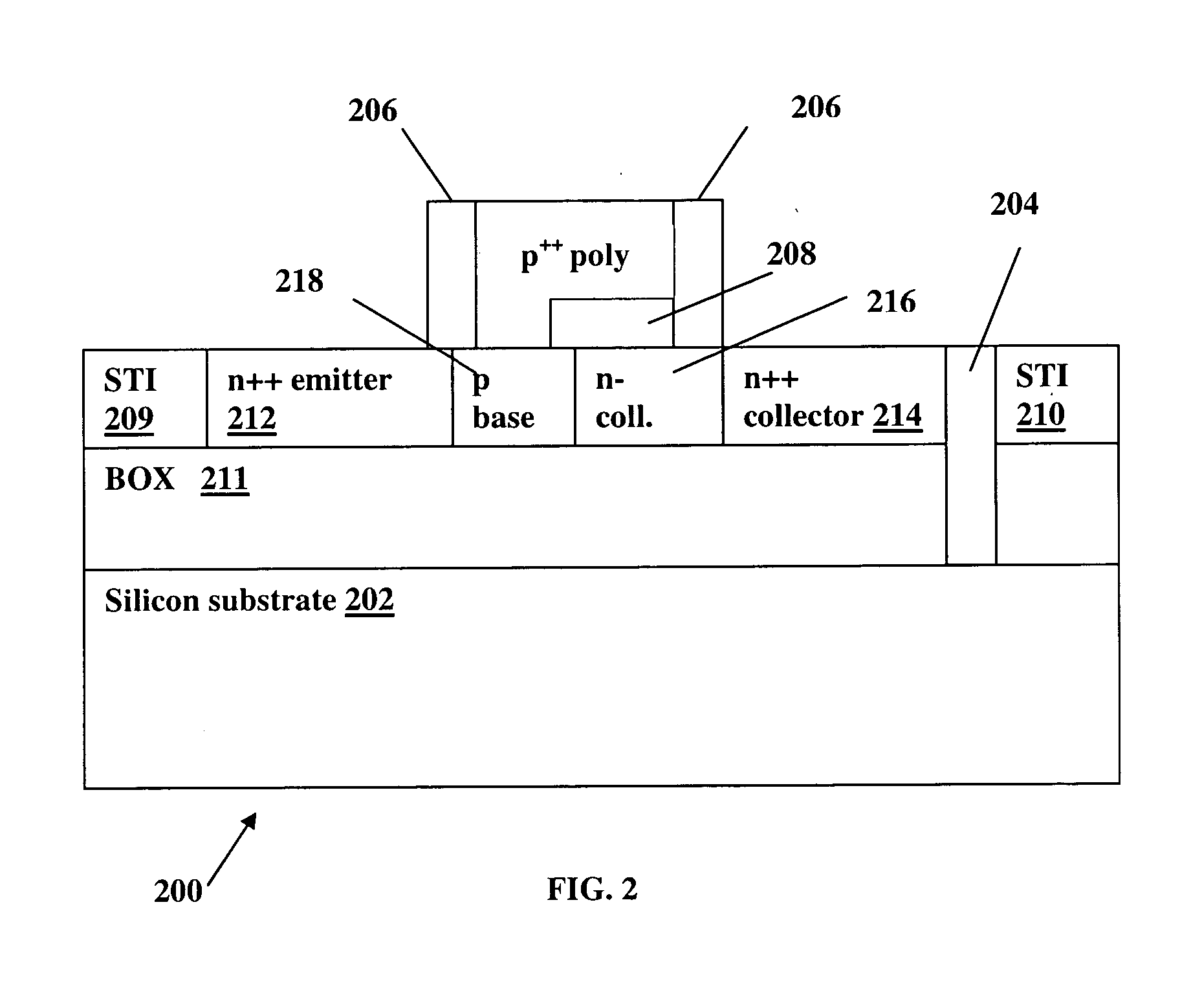
[0015] Referring to FIG. 2, we show a lateral BJT on SOI structure 200 according to the invention. Lateral BJT 200 comprises a Silicon substrate 202, an n-type collector 216, an n++ collector 214, a p-type base 218, an n-type emitter 212 (heavily doped), and a metal or polysilicon connection 204 connecting the n++ collector 214 to the substrate 202. Oxide regions 206 and 208 provide isolation. The BJT 200 further comprises STI regions 209 and 210, and a BOX layer 211. The connection path 204 can comprise any material that conducts the heat generated by the collector to the substrate 202 or anywhere else having a lower temperature than the collector.
[0016] We now briefly discuss a simulated device having a single-finger, n++ poly emitter with width (WE) of 100 nm, a uniform base doping profile (NB) of 2e18 cm−3 and a collector doping concentration (Nc) of 1e17 cm−3. The base width is 80 nm. The SOI thickness (TSOI) is 100 nm and the BOX thickness (TBOX) is 200 nm for the SOI devices....
third embodiment
[0018] Referring to FIG. 4, we show a complementary BiCMOS on SOI integrated transistor structure 400 with vertical BJT and the heat drainage, according to a The substrate for the BJT devices is isolated by p-wells and n-wells. Structure 400 comprises complementary BJTs 402 (pnp) and 404 (npn) and complementary MOSFETs (metal-oxide field-effect transistors): NMOS 406 and pMOS 408, with well isolation and heat drainage. The heat draining is accomplished with heat conductive paths from the collector of the pnp BJT 402 to the p-well and from the collector of the npn BJT 404 to the n-well.
[0019] Referring to FIG. 5, we show a method 500 for constructing a bipolar transistor comprising a collector, a base, and an emitter, all located over a substrate according to another embodiment of the invention. The method 500 comprises steps of: creating a collector layer over the substrate 502; etching a path through the collector layer to the substrate 504; filling the path with a heat-conductive...
PUM
 Abstract
Description
Claims
Application Information
 - R&D Engineer
- R&D Manager
- IP Professional
- Industry Leading Data Capabilities
- Powerful AI technology
- Patent DNA Extraction
Browse by: Latest US Patents, China's latest patents, Technical Efficacy Thesaurus, Application Domain, Technology Topic, Popular Technical Reports.
© 2024 PatSnap. All rights reserved.Legal|Privacy policy|Modern Slavery Act Transparency Statement|Sitemap|About US| Contact US: help@patsnap.com