
Microelectronic assemblies having low profile connections

a microelectronic and low-profile technology, applied in the direction of electrical equipment, semiconductor devices, semiconductor/solid-state device details, etc., can solve the problems of increasing the stress of the leads, affecting the flexibility of the dielectric layer, and increasing the height of the connection between the leads and contacts, so as to achieve low stress on the conductive elements

Inactive Publication Date: 2006-12-07
TESSERA INC
View PDF24 Cites 0 Cited by
  • Summary
  • Abstract
  • Description
  • Claims
  • Application Information

AI Technical Summary

Benefits of technology

This approach reduces stress on conductive elements by allowing the dielectric layer to flex more freely, enhancing the reliability and stability of microelectronic assemblies during thermal cycles.

Problems solved by technology

However, the larger the dielectric layer, the more stress the leads experience.
This is compounded by the presence of bonding material between the contacts and the leads, which interferes with the flexibility of the dielectric layer.
However, some connections incorporate a significant amount of bonding material, which adds to the height of the connection between the leads and contacts, and impacts the reliability of the assembly.

Method used


Image

  • Microelectronic assemblies having low profile connections
  • Microelectronic assemblies having low profile connections
  • Microelectronic assemblies having low profile connections

Examples


Embodiment Construction

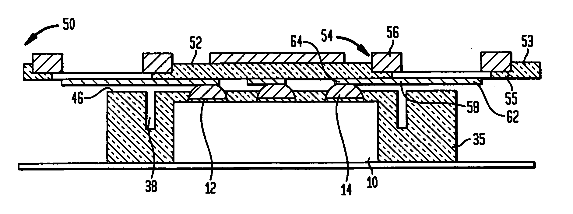
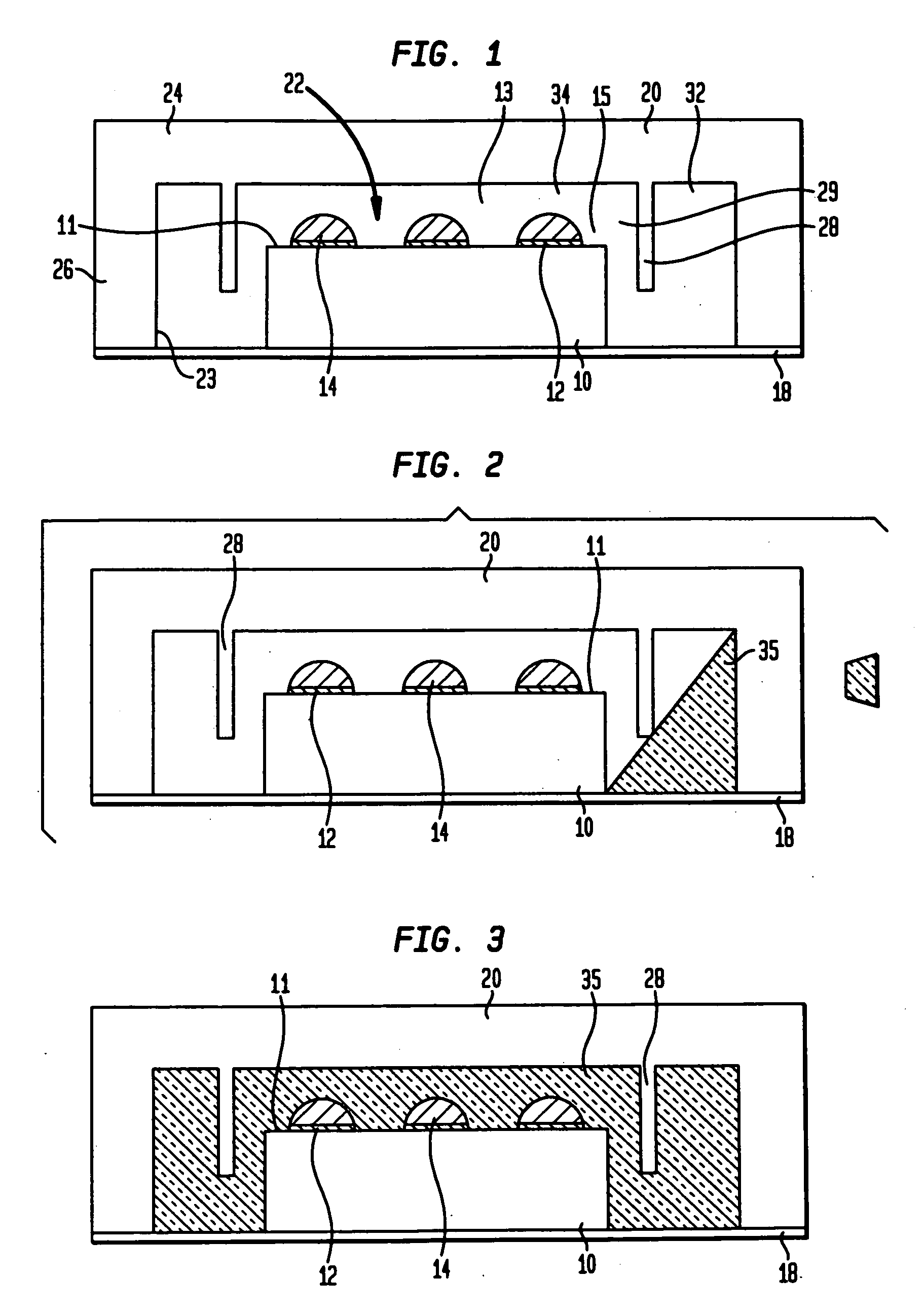
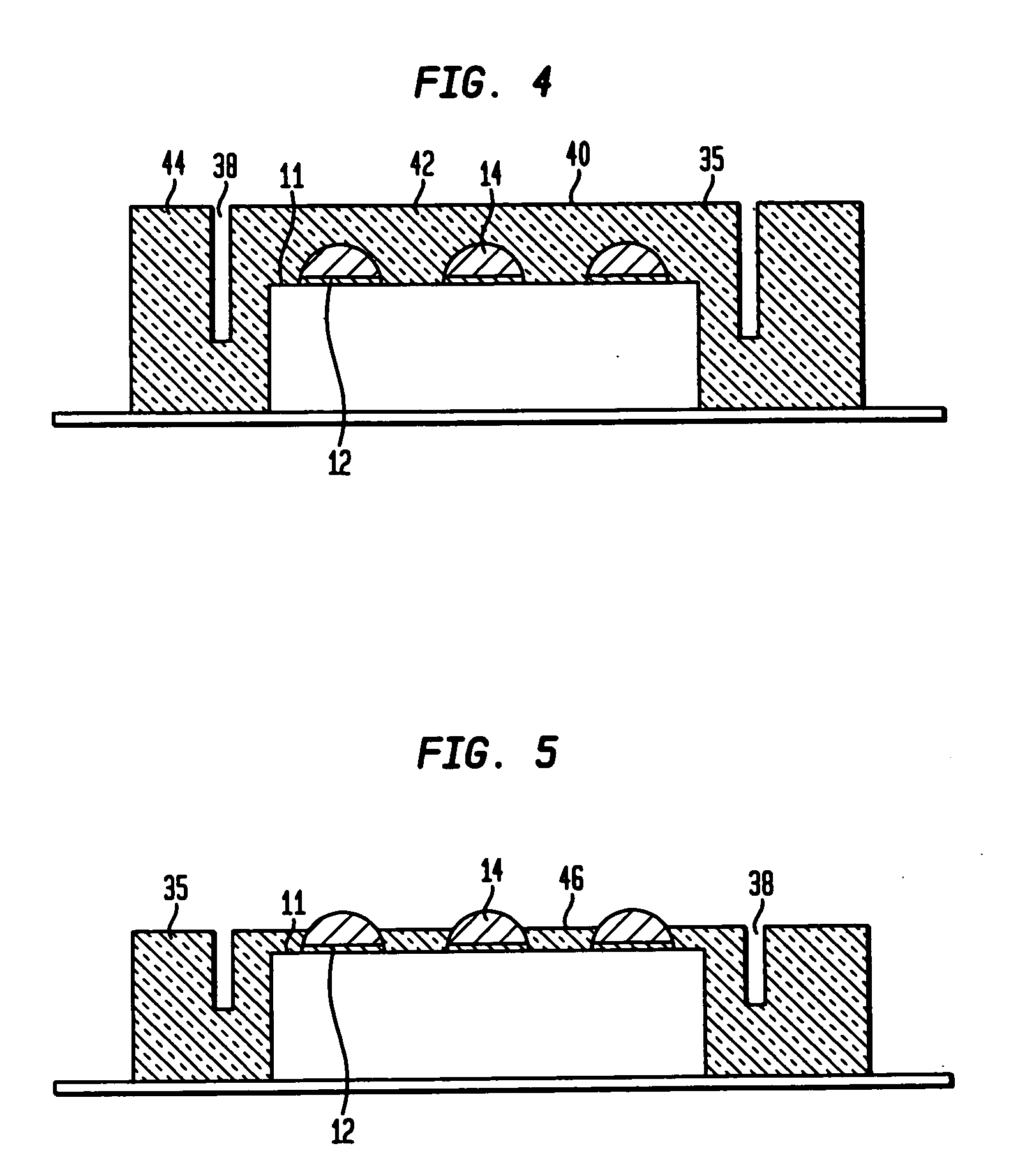
[0058] The method of forming a microelectronic assembly in accordance with one embodiment of the invention is shown in FIGS. 1-9. As shown in FIG. 1, the microelectronic element 10 has a first surface 11 with a plurality of conductive features including contacts 12 exposed at the first surface. The microelectronic element 10 has a central region 13 lying inwardly of a peripheral region 15. In the cross-sectional view of FIG. 1, only three contacts 12 are shown. However, typically a microelectronic element 10 has many contacts that are arranged on the first surface 11 in the central region 13, or in the peripheral region 15 of the microelectronic element 10, or both. The arrangement of the contacts on the microelement element 10 is not critical to the invention.

[0059] The conductive features also include, in certain embodiments, protrusions, such as masses of bonding material, such as solder. The protrusions may comprise bumps or posts or other members attached to the contacts 12. T...


PUM


Abstract

A microelectronic assembly includes a first microelectronic element having a first face and contacts accessible at the first face, and a layer of a dielectric material having a bottom surface contacting the first microelectronic element, a top surface facing away from the first microelectronic element and holes extending between the top and bottom faces in alignment with the contacts on the first microelectronic element. The assembly includes conductive protrusions extending through the holes to the contacts, the conductive protrusions projecting beyond the top surface of the dielectric layer. The assembly also has a second microelectronic element having a first surface with conductive elements being accessible at the first surface thereof, the second microelectronic element being assembled with the first microelectronic element so that the contacts of the second microelectronic element are connected with the conductive protrusions and the top surface of the dielectric layer is spaced from the first surface of the second microelectronic element.

Description

CROSS-REFERENCE TO RELATED APPLICATIONS [0001] The present application is a continuation of U.S. patent application Ser. No. 10 / 699,328, filed Oct. 31, 2003, which claims the benefit of U.S. Provisional Application Ser. No. 60 / 426,478 filed Nov. 13, 2002, the disclosures of which are hereby incorporated by reference herein.FIELD OF THE INVENTION [0002] The present invention relates to methods of making microelectronic assemblies and to microelectronic assemblies. BACKGROUND OF THE INVENTION [0003] Microelectronic elements are typically packaged and assembled with a microelectronic component to facilitate connection to external circuitry. Heat is generated in use, as well as during manufacturing operations such as, for example, bonding. When heat is generated within the assembly, the various parts of the assembly expand and contract according to the coefficient of thermal expansion for the particular part. Incorporating various materials having different coefficients of thermal expan...

Claims


Application Information

Patent Timeline
Patent Type & Authority Applications(United States)
IPC IPC(8): H01L21/00H01L21/44H01L23/31H01L23/485H01L23/498H01L23/538
CPCH01L23/3128H01L23/3135H01L24/13H01L23/49816H01L23/49827H01L23/4985H01L23/5389H01L24/10H01L2224/13099H01L2924/01013H01L2924/01022H01L2924/01029H01L2924/01079H01L2924/01082H01L2924/01322H01L2924/01005H01L2924/01006H01L2924/01024H01L2924/01033H01L2924/014H01L2224/73204H01L2224/81193H01L2224/8193H01L2924/00H01L2224/13022H01L2224/13H01L2224/05022H01L2224/05001H01L2224/05572H01L24/16H01L2224/0615H01L2224/05644H01L2924/00014H01L2224/05647H01L2224/05655H01L2224/05666H01L2224/05671H01L2224/05124
Inventor WARNER, MICHAELBEROZ, MASUDLIGHT, DAVIDLI, DELINCASTILLO, DENNISWANG, HUNG-MINGSMITH, JOHN W.
Owner TESSERA INC
Learn More