Light-emitting device, method for driving the same driving circuit and electronic apparatus

Active Publication Date: 2006-11-30
ELEMENT CAPITAL COMMERCIAL CO PTE LTD
View PDF18 Cites 40 Cited by
  • Summary
  • Abstract
  • Description
  • Claims
  • Application Information

AI Technical Summary

Benefits of technology

[0008] An advantage according to an aspect of the present invention is to provide a driving method of the electronic circuit capable of sufficiently correcting the variance of the theshold voltage of the driving transistor without extending the writing period, a driving circuit, a light-emitting device and an electronic apparatus as described above.
[0014] In this case, in the plurality of correcting periods, the first switching unit is turned on, whereby the driving transistor acts as a diode. Then, the gate potential corresponding to the theshold voltage of the driving transistor is held in the holding unit. Further, since the reference voltage is supplied to the other end of the capacitor element in the last correcting period, while the data voltage is supplied to the other end of the capacitor element, the voltage potential of the gate to correct the theshold voltage of the driving transistor is supplied at the time when the writing period is terminated. Herewith, when the unbalance of the theshold voltage of each driving transistor turns up, the brightness unbalance can be prevented all over the screen through the correcting In addition, the second switching unit may be turned on while the reference voltage is supplied to the data line in the whole correcting period.
[0018] In addition, it is desirable to commonly establish the initialization period to all of the plurality of pixel circuits. In this case, since the gate potential of the driving transistor can be set as the initialization voltage potential for all of the pixel circuits if the initialization is once implemented, the processing can be simply and easily performed. More concretely, when the period requiring to select all of the plurality of scanning lines is set to one-frame period, it is desirable to establish the one-frame period once a one-frame period.
[0019] Further, with reference to the driving method or the light-emitting device as described above, it is desirable to establish the light-emitting period to supply the driving current to the light-emitting element after the writing period is terminated. In this case, it becomes possible that the light-emitting element is light-emitted when the unbalance of the driving current is corrected. On addition, it is desirable that the light-emitting period is divided into the plurality of periods. In this case, the light-emitting period is diversified to prevent flicker.
[0023] According to the aspect of the invention, since the correcting is implemented in the plurality of the correcting period, whereby although the theshold voltage of the driving transistor is spread to the manufacturing process, the brightness unbalance can be improved. Besides, since the reference voltage and data voltage are supplied to the data line by time-sharing, to be load to the pixel circuit, it is not particularly necessary to provide the wire for supplying the reference voltage to each pixel circuit. As the result, the area of the light-emitting element can be enlarged in the pixel circuit, whereby the aperture ratio can be improved.

Problems solved by technology

In this configuration, there is represented the problem that as the threshold voltage characteristic of the driving transistor fluctuates, the brightness of the OLED element for each pixel is various, whereby the visual quality is deteriorated.
However, the first period and second period may be not only continuous, but also discontinuous.

Method used


Image

  • Light-emitting device, method for driving the same driving circuit and electronic apparatus
  • Light-emitting device, method for driving the same driving circuit and electronic apparatus
  • Light-emitting device, method for driving the same driving circuit and electronic apparatus

Examples


Embodiment Construction

Construction of Light-Emitting Device

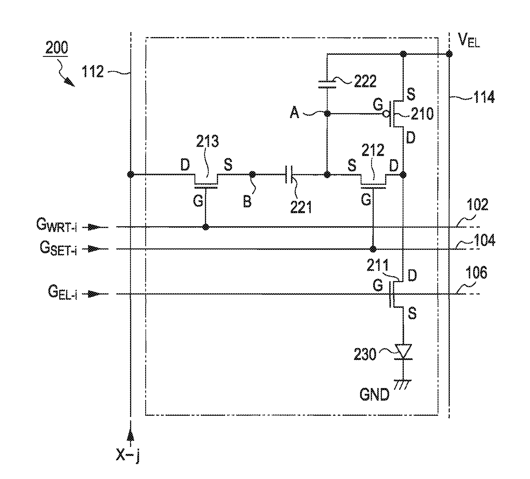
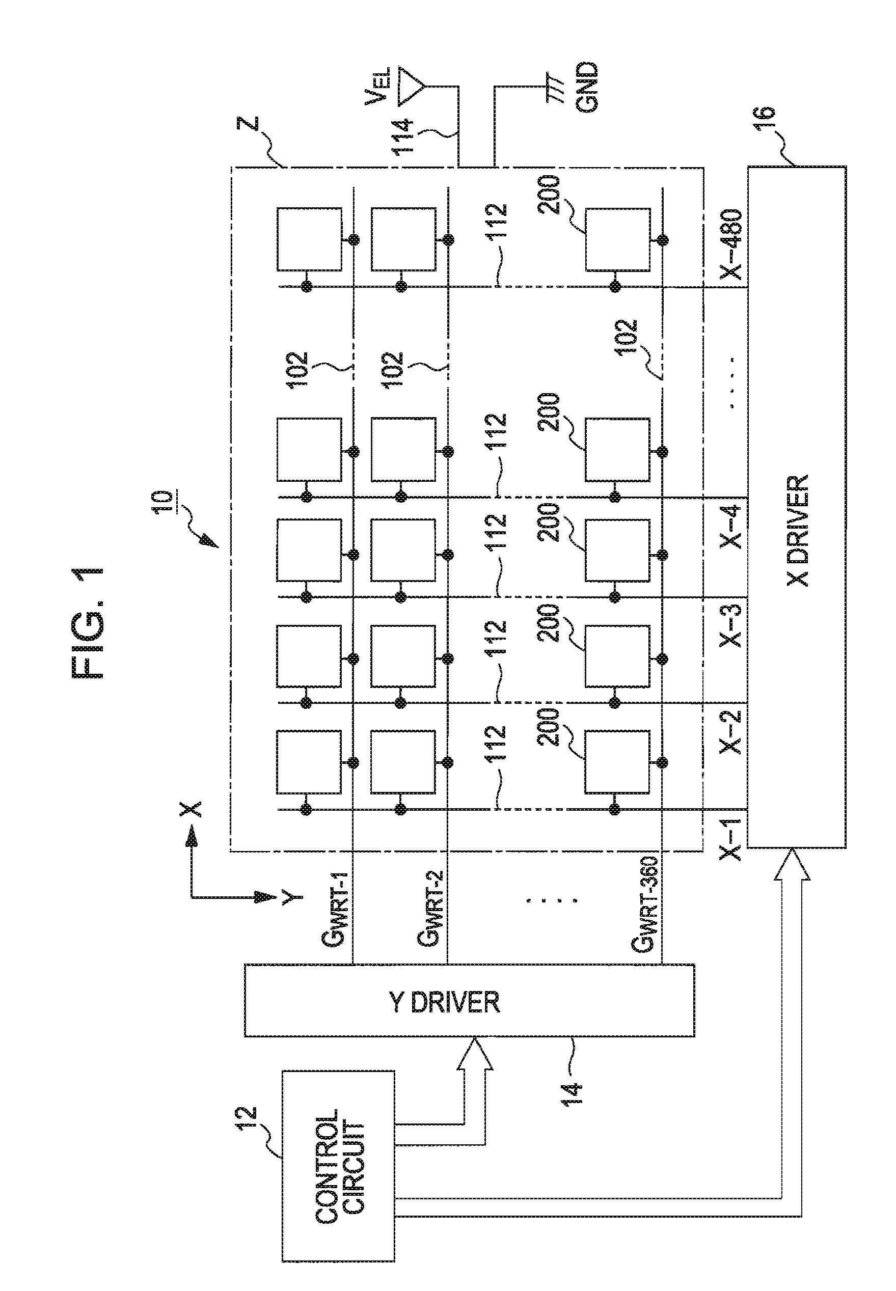
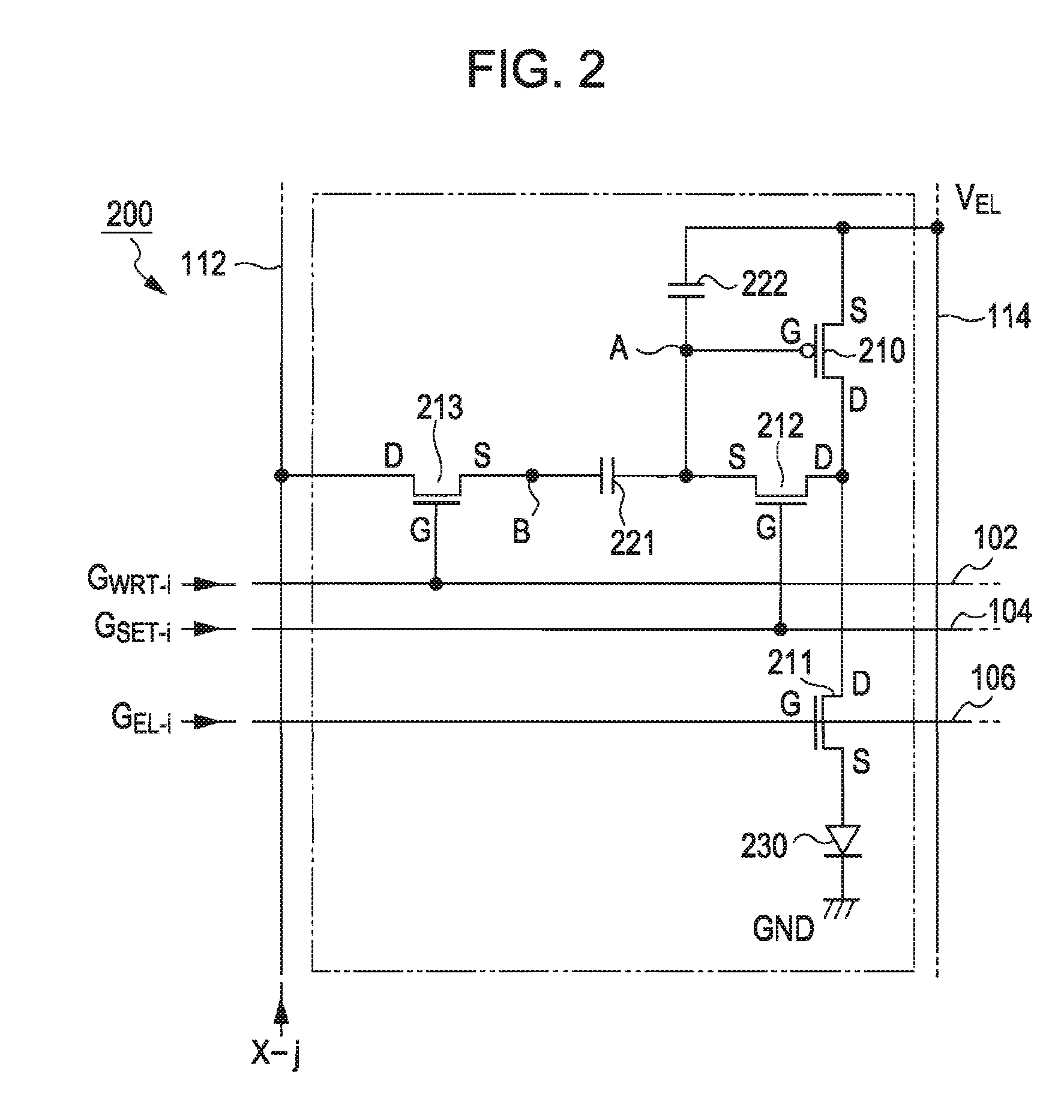
[0046]FIG. 1 is a block diagram showing the construction of a light-emitting device according to an embodiment of the invention and FIG. 2 is a circuit diagram showing a pixel circuit. As shown in FIG. 1, a light-emitting device 10 has a light-emitting zone Z in which a plurality pixel circuits 200 are arranged in a matrix. In the light-emitting zone Z, a plurality of scanning lines 102 are extensively provided in a crosswise direction (X direction), while a plurality of data lines (signal lines) 112 are extensively provided in a lengthwise direction (Y direction) as shown in FIG. 1. And, the pixel circuits (electronic circuits), respectively, 200 are provided so as to correspond to each intersection of the scanning lines 102 and the data lines 112.

[0047] For the convenience of description, in this embodiment, the number (number of lines) of scanning lines 102 in the light-emitting zone is set to ‘360’ and the number of (number of rows) is set...


PUM


Abstract

A method for driving a light-emitting device in which a plurality of pixel circuits are arranged in correspondence with the intersection of a plurality of scanning lines and a plurality data lines, the pixel circuit having a light-emitting element and a driving transistor that controls the current amount of a driving current flowing the light-emitting device, comprises repeating the process within unit period including a first period and a second period following the first period, wherein the second period process includes selecting one scanning line of the plurality of scanning lines, and supplying and holding a data voltage corresponding to the luminance of the light-emitting element to a gate of the driving transistor via the data lines with respect to the plurality pixel circuits connected the selected scanning lines, and wherein the first period process includes selecting two or more scanning lines of the plurality of scanning lines, and correcting the unbalance of the driving current output from the driving transistor in the plurality of pixel circuits connected to the selected scanning lines.

Description

[0001] This application claims the benefit of Japanese Patent-Application No. 2505-151895, filed May 25, 2005. The entire disclosure of the prior application is hereby incorporated by reference herein its entirety. BACKGROUND [0002] 1. Technical Field [0003] The present invention relates to a light-emitting device having a light-emitting element such as an organic light-emitting element, a method for driving the same, a driving circuit and an electronic apparatus. [0004] 2. Related Art [0005] Recently, an Organic Light-Emitting Diode (hereinafter, referred to as ‘OLED element’) called an organic electro-luminescent element or a light-emitting polymer element as a next-generation light-emitting diode replacing a liquid crystal element has gotten a lot of attention. Since this OLED element is self-luminous type, it shows low dependence on the view angle and does not need a backlight or reflected light, thereby having excellent characteristics as a display panel such as the reduction o...

Claims


Application Information

Patent Timeline
IPC IPC(8): G09G3/30H05B44/00
CPCG09G3/3233G09G3/3291G09G2300/0465G09G2300/0819G09G2300/0852G09G2360/144G09G2310/0262G09G2320/0233G09G2320/0247G09G2320/043G09G2300/0861G09G3/30G09G3/20
Inventor TAKAHASHI, KASORIKANDA, EIJIOZAWA, TOKURO
Owner ELEMENT CAPITAL COMMERCIAL CO PTE LTD
Why Eureka
Try Eureka