
Multi element, multi color solid state LED/laser

a solid-state led/laser, multi-element technology, applied in the direction of lasers, semiconductor laser arrangements, semiconductor lasers, etc., can solve the problems of increasing costs, unable to generate white light from active layers, and devices that require complicated control electronics, so as to achieve efficient emitted light, efficiently produce blue and green light, and effectively change the color of light emitted from the overall device

Inactive Publication Date: 2006-11-16
CREE INC
View PDF11 Cites 24 Cited by
  • Summary
  • Abstract
  • Description
  • Claims
  • Application Information

AI Technical Summary

Benefits of technology

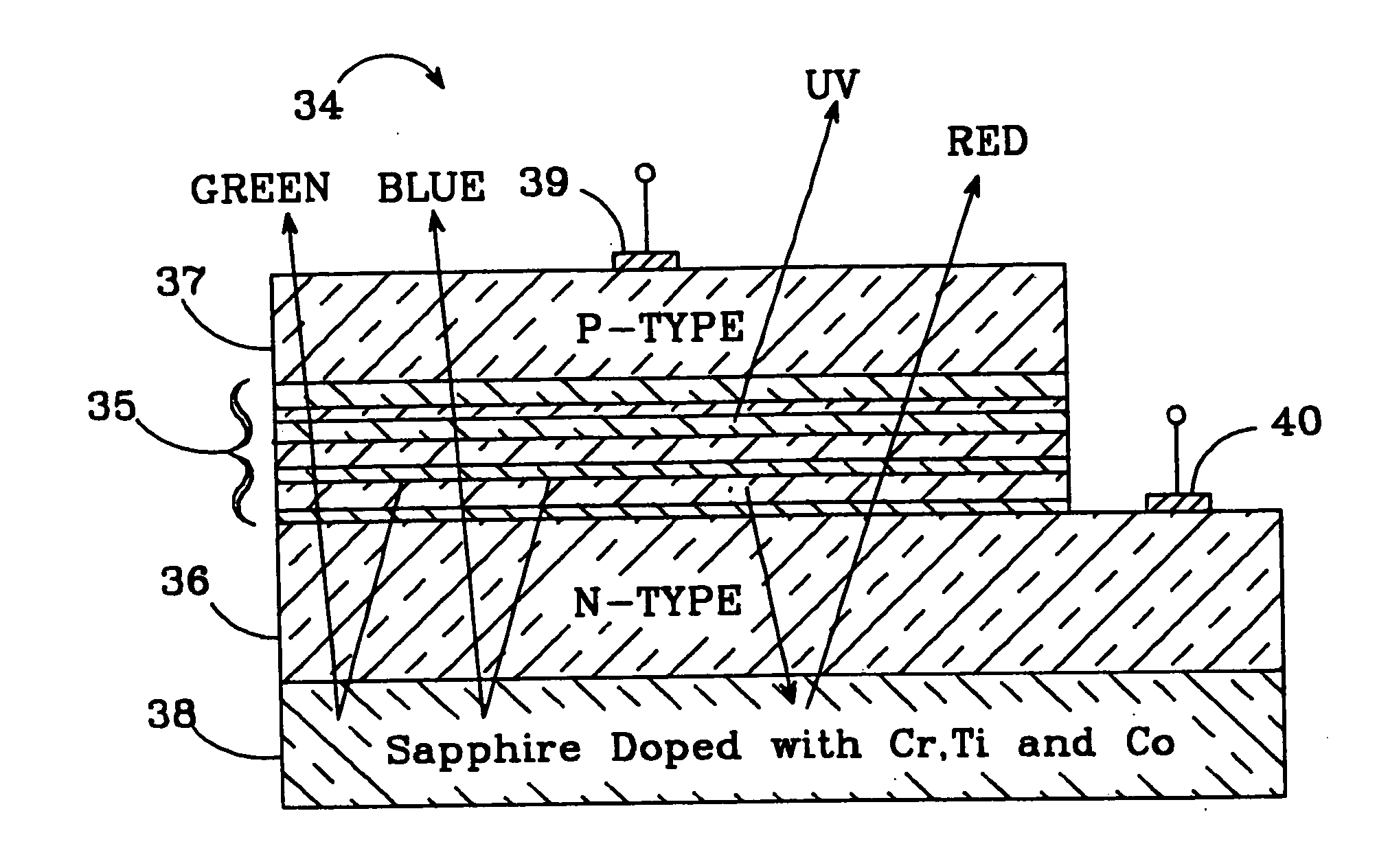
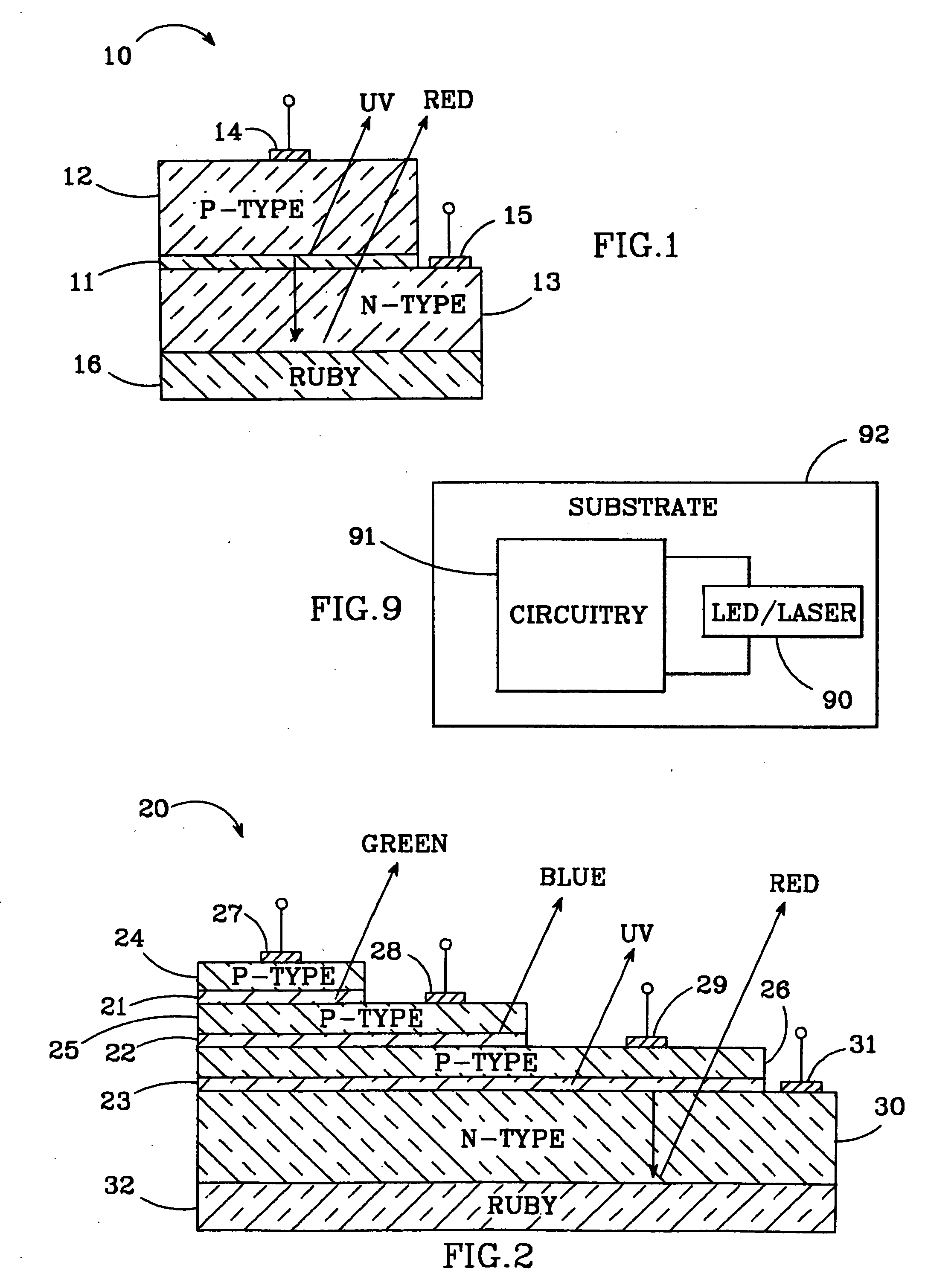
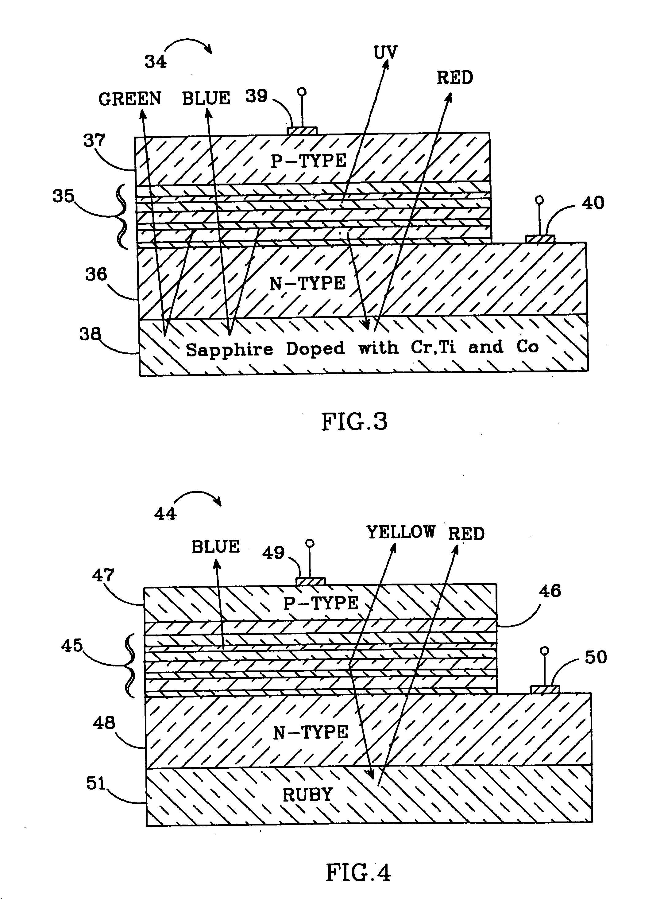
The present invention provides new LEDs and solid state lasers that use rare earth or transition elements doped onto substrates. These LEDs and lasers produce new colors of light by using the light absorption and emission properties of the doped substrate. The LEDs can have multiple emitting layers or substrates doped with different elements, allowing for the production of different colors. The LEDs can also be tuned to emit different colors by manipulating the current applied to the various layers. The doped substrate approach can also be used in solid state lasers to more efficiently produce blue and green light. The invention can create more temperature resistant red lasers and different types of lasers emitting different colors of light.

Problems solved by technology

One disadvantage of conventional LEDs is that they cannot generate white light from their active layers.
One disadvantage of this approach is that it requires the use of multiple LEDs to produce a single color of light, increasing costs.
In addition, different colors of light are often generated from different types of LEDs which can require complex fabrication to combine in one device.
The resulting devices can also require complicated control electronics since the different diode types can require different control voltages.
Long term wavelength and stability of these devices is also degraded by the different aging behavior of the different LEDs.
However, the addition of the phosphor results in a more complex LED that requires a more complex manufacturing process.
In addition, the net light emitting efficiency is reduced due to the absorption in the phosphor and the stokes shift from blue to yellow.
Another disadvantage of most conventional LEDs is that they are less efficient at converting current to light compared to filament lights.
However, conventional blue LEDs operate from a relatively low supply current that results is a light that is too dim for many lighting applications.
This problem is compounded by the absorption of some of the blue light by the downconverting material used to generating white light from blue.
At this current, LEDs become very hot and any material surrounding the LED will also become hot.
The heat can damage the downconverting material surrounding the LED, degrading its ability to downconvert the LED's light.
The heat can also present a danger of burning objects that are near or in contact with the LED.
Another disadvantage of conventional LEDs is that they only emit one color of light.
In applications such as displays or television screens, this can result in a prohibitive number of LEDs and can require complex control electronics.
However, conventional solid state lasers cannot efficiently emit green and blue light.
Red emitting solid state lasers are more common, but their performance degrades with temperature and if the temperature reaches a high enough point, the laser will stop emitting light.

Method used


Image

  • Multi element, multi color solid state LED/laser
  • Multi element, multi color solid state LED/laser
  • Multi element, multi color solid state LED/laser

Examples


Embodiment Construction

[0031]FIG. 1 shows a single active layer nitride based LED 10 constructed in accordance with the invention. It has an InGaN active layer 11 which emits UV light, sandwiched between two oppositely doped GaN layers 12 and 13. The top layer 12 is usually p-type GaN and bottom layer 13 is usually n-type GaN although the new LED would also work if the layers were reversed. The p-type layer and n-type layers have respective contacts 14 and 15, each having a lead to apply a bias across the active layer 11, causing it to emit light omnidirectionally. The entire LED is grown on a sapphire (Al2O3) substrate doped with chromium (Cr), which creates ruby. Ruby is commercially available from companies such as Union Carbide in a form that can be used for substrates on solid state devices. The LED can be grown on the substrate by many known methods with the preferred method being Metal Organic Chemical Vapor Deposition (MOCVD).

[0032] Some of the light emitted from active layer 11 will pass through...


PUM


Abstract

A light emitting diode (LED) grown on a substrate doped with one or more rare earth or transition element. The dopant ions absorb some or all of the light from the LED's active layer, pumping the electrons on the dopant ion to a higher energy state. The electrons are naturally drawn to their equilibrium state and they emit light at a wavelength that depends on the type of dopant ion. The invention is particularly applicable to nitride based LEDs emitting UV light and grown on a sapphire substrate doped with chromium. The chromium ions absorb the UV light, exciting the electrons on ions to a higher energy state. When they return to their equilibrium state they emit red light and some of the red light will emit from the LED's surface. The LED can also have active layers that emit green and blue and UV light, such that the LED emits green, blue, red light and UV light which combines to create white light. Alternatively, it can have one active layer and grown on a sapphire substrate doped with Cr, Ti, and Co such that the substrate absorbs the UV light and emits blue, green, and red light. The invention is also capable of providing a tunable LED over a variety of color shades. The invention is also applicable to solid state laser having one or more active layers emitting UV light with the laser grown on a sapphire substrate doped with one or more rare earth or transition elements.

Description

[0001] The following application is a utility application for provisional application No. 60 / 166,444 to Denbaars et al., which was filed on Nov. 19, 1999. BACKGROUND OF THE INVENTION [0002] 1. Field of the Invention [0003] This invention relates to solid state light emitting diodes (LEDs) and lasers that can emit various colors of light, including white. [0004] 2. Description of the Related Art [0005] Light emitting diodes (LEDs) are an important class of solid state devices that convert electric energy to light. They generally comprise one or more active layers of semiconductor material sandwiched between oppositely doped layers. When a bias is applied across the doped layers, holes and electrons are injected into the active layer where they recombine to generate light. Light is emitted omnidirectionally from the active layer and from all surfaces of the LED. The useful light is generally emitted in the direction of the LED's top surface, which is usually p-type. [0006] One disadva...

Claims


Application Information

Patent Timeline
Patent Type & Authority Applications(United States)
IPC IPC(8): H01L33/00H01L21/00H01L25/075H01L27/15H01L33/08H01L33/30H01L33/34H01L33/50H01S5/026H01S5/40
CPCH01L25/0756H01S5/32341H01L27/153H01L33/08H01L33/30H01L33/343H01L33/504H01S3/0627H01S3/0941H01S3/09415H01S3/1623H01S3/1628H01S5/0206H01S5/0287H01S5/1032H01S5/183H01S5/18361H01L27/15H01L2924/0002H01L33/502H01L2924/00
Inventor DENBAARS, STEVEN P.TARSA, ERIC J.MACK, MICHAELKELLER, BERNDTHIBEAULT, BRIAN
Owner CREE INC
Learn More