
Chemical mechanical polishing compositions for step-ll copper line and other associated materials and method of using same

a technology of chemical mechanical polishing and composition, which is applied in the direction of polishing compositions with abrasives, other chemical processes, chemistry apparatus and processes, etc., can solve the problems of unwanted copper dishing and/or dielectric material erosion, and achieve the effect of reducing the occurrence of copper dishing and dielectric or oxide erosion

Inactive Publication Date: 2006-11-09
ADVANCED TECH MATERIALS INC
View PDF19 Cites 79 Cited by
  • Summary
  • Abstract
  • Description
  • Claims
  • Application Information

AI Technical Summary

Benefits of technology

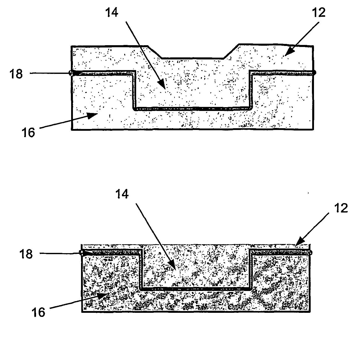
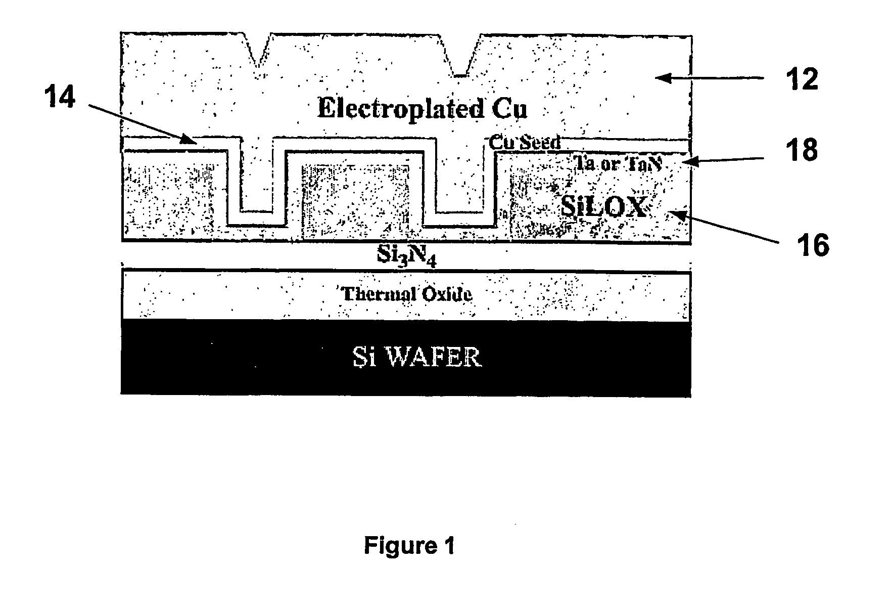
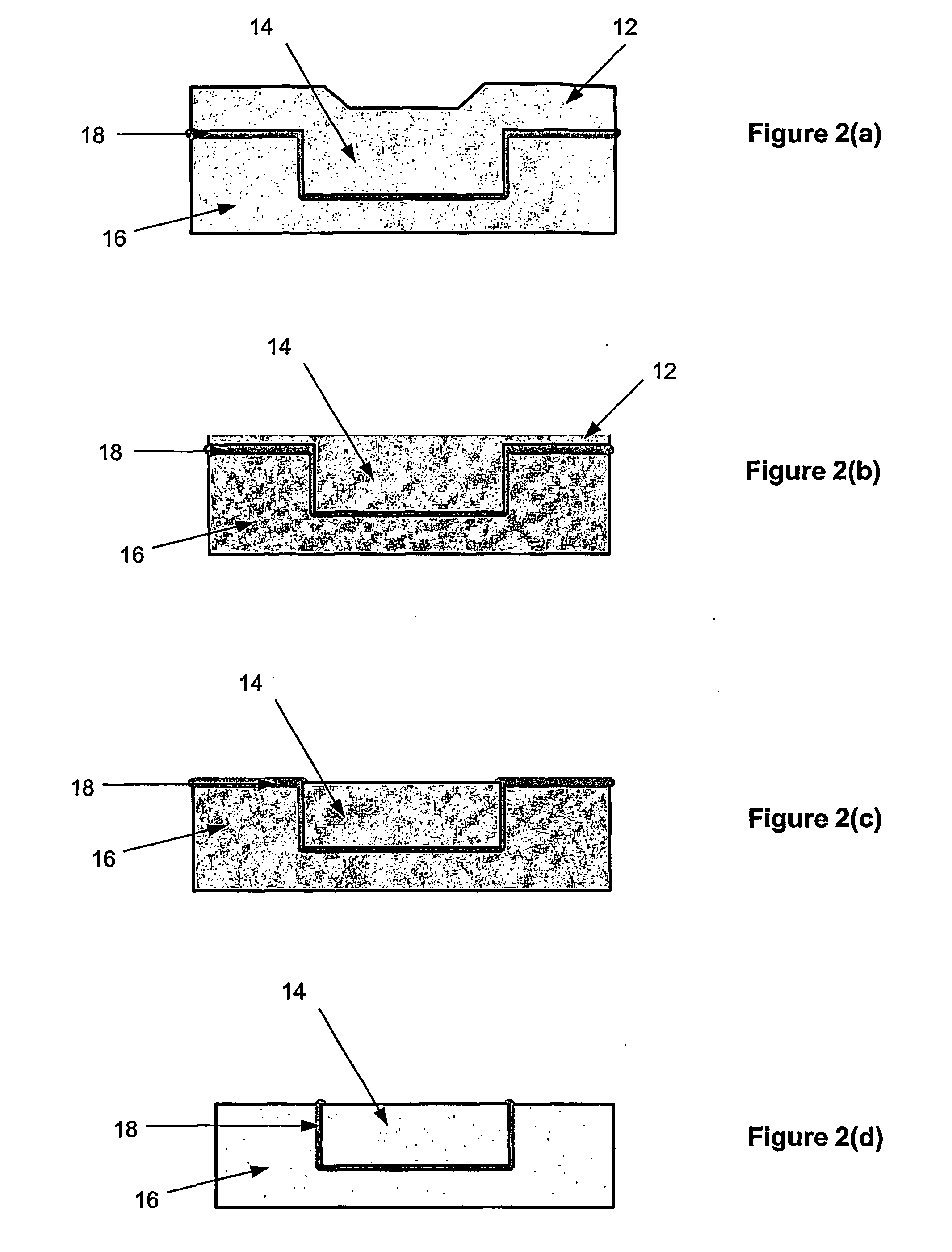
[0014] The present invention relates to a CMP slurry composition and process designed to planarize barrier materials such as tungsten nitride, tantalum, tantalum nitride, silicon doped tantalum nitride, titanium nitride and silicon doped titanium nitride, which are associated with a copper CMP process step. And as broadly disclosed herein, the CMP slurry composition, when used in a copper damascene planarization step, reduces the occurrence of copper dishing and dielectric or oxide erosion while controlling the rates at which both dielectric and barrier materials are removed.

Problems solved by technology

If appropriate material removal selectivity is not maintained, unwanted dishing of copper and / or erosion of the dielectric material may occur.

Method used


Image

  • Chemical mechanical polishing compositions for step-ll copper line and other associated materials and method of using same
  • Chemical mechanical polishing compositions for step-ll copper line and other associated materials and method of using same
  • Chemical mechanical polishing compositions for step-ll copper line and other associated materials and method of using same

Examples


example 1

[0081] Bulk copper overburden was removed from an 854 Reticle (854 CMP025) wafer manufactured by Sematech, Inc. using a Step I slurry composition for bulk copper removal. Copper lines were polished using the Step II slurry composition outlined in Row 2 of Table 1 hereinabove. Careful inspection with an optical microscope showed that all liner was removed evenly and uniformly within 30 s. To ensure that the Cu lines were electrically isolated and shorts eliminated, a thin layer of SiO2 (200-300 Å) was removed as well.

[0082]FIG. 4 shows a graph plotting the step height reduction from the dielectric field area into the copper line array pre and post liner polish with the CMP slurry composition outlined in Row 2 of Table 1. In addition to removing the Ta liner the Step II CMP composition also planarized the wafer surface. Dishing and Erosion measures the step height from the field area, unpatterned, open areas of the chip, into the copper line arrays. The step height from pre to post l...

example 2

[0083]FIG. 5 shows a plot of removal rates for a thin film of Ta (liner material) and SiO2 (dielectric material) present on a Si wafer surface as a function of weight percent concentration of boric acid component in a CMP composition. The composition comprising 13 wt. % silica, 10 wt. % hydrogen peroxide, 0.1 wt % BTA, pH 6.0 and varying wt % boric acid. At low boric acid concentrations the material removal rates as shown are fairly low, too low to insure high wafer throughput in IC chip manufacturing. Adding boric acid to the slurry increases both removal rates. However, the Ta removal rate shows a stronger increase with increasing boric acid concentration. At 0.4% wt boric acid the increase in the SiO2 removal rate has saturated, but the Ta removal rate is still further increasing. This shows, that with the current Step 2 formulation, containing boric acid, the polishing process is highly tunable by the boric acid content. Thus depending on the specific needs of a particular integ...


PUM

PropertyMeasurementUnit
wt. %aaaaaaaaaa
mean sizeaaaaaaaaaa
timeaaaaaaaaaa

Abstract

A CMP composition and process for planarization of a semiconductor wafer surface having a copper barrier layer portion, said composition comprising an oxidizing agent, a boric acid component, and an abrasive.

Description

FIELD OF THE INVENTION [0001] The present invention relates to a chemical mechanical polishing slurry for surfaces of a semiconductor wafer, and more particularly, to a chemical mechanical polishing slurry and a method for using the slurry to remove and polish copper, barrier materials and dielectric materials layered on semiconductor wafer surfaces. DESCRIPTION OF THE RELATED ART [0002] Semiconductor wafers are used to form integrated circuits. The semiconductor wafer includes a substrate, such as silicon, into which regions are patterned for deposition of different materials having insulative, conductive or semi-conductive properties. [0003] In order to obtain the correct patterning, excess material used in forming the layers on the substrate must be removed. Further, to fabricate functional and reliable circuitry, it is important to have a flat or planar semiconductor wafer surface. Thus, it is necessary to remove and / or polish certain surfaces of a semiconductor wafer. [0004] Ch...

Claims


Application Information

Patent Timeline
Patent Type & Authority Applications(United States)
IPC IPC(8): C09K13/00H01L21/461B44C1/22C09G1/02H01L21/321
CPCC09G1/02C09K3/1463H01L21/7684C23F3/06H01L21/3212C23F3/04
Inventor WRSCHKA, PETERBERNHARD, DAVIDBOGGS, KARLDARSILLO, MICHAEL
Owner ADVANCED TECH MATERIALS INC
Learn More