
Hard mask arrangement

a technology of hard masks and masks, applied in the field of hard masks, can solve the problems of high cost of masks used in optical lithography techniques and the complexity of the lithography tool used at these reduced feature sizes, and the development of such materials and methods may be in turn very costly, and achieve the effect of cost-effectiveness

Inactive Publication Date: 2006-10-19
FEHLHABER RODGER +1
View PDF15 Cites 232 Cited by
  • Summary
  • Abstract
  • Description
  • Claims
  • Application Information

AI Technical Summary

Benefits of technology

[0009] In order to reduce the pitch for forming a hard mask, spacer structures may be produced from a layer formed by conformal turn-off. The structures extending over the substrate and adjoining the spacers are removed after spacer formation has been effected. In other techniques, two hard mask layers are deposited so that one layer lies above another, and a photoresist layer is applied above the second hard mask layer. Firstly, a region of the second hard mask layer that is uncovered by means of the patterned photoresist is removed in such a way that the portions of the second hard mask layer which remain beneath the photoresist layer is subsequently used as an etching mask for etching the first hard mask layer. The second hard mask layer is trimmed and the uncovered regions of the first hard mask layer are subsequently etched using the remaining material of the second hard mask layer as a hard mask. The patterned first hard mask layer is subsequently trimmed in turn.
[0007] Resolution enhancement techniques (“RET”) are used to produce structures having the corresponding desired size in the most critical—in terms of resolution—layers of a wafer of the 65 nm technology node, and to thus improve a customary 193 nm lithography. In particular, for the production of very small gate structures with precise control of the critical dimension (“CD”), the only suitable approach at the present time is to be seen in the use of alternating phase shift masks (“altPSM”), in association with double exposure. However, the double exposure and the alternating phase shift masks dramatically increase the process costs.

Problems solved by technology

The chemistry used for a photoresist material, the production of mask(s) used in the optical lithography techniques and the complexity of the lithography tool used may be cost-intensive at these reduced feature sizes.
Such materials have not heretobefore been developed, despite considerable development efforts.
The development of such materials and methods may be in turn very costly.
A new and expensive infrastructure may be required for the production of masks for 157 nm lithography methods.
Finally, the tool, that is to say the apparatus which carries out the lithography method using light having the wavelength λ=157 nm, is itself expensive and requires considerable development work.
However, the double exposure and the alternating phase shift masks dramatically increase the process costs.
However, the reliability may be very low since, on account of the process conditions present in the context of the plasma CVD method, the photoresist structure is destroyed or thermally treated in such a way that it can subsequently be removed only with great difficulty and with possible impairment of the rest of the circuit structure formed.

Method used


Image

  • Hard mask arrangement
  • Hard mask arrangement
  • Hard mask arrangement

Examples


Embodiment Construction

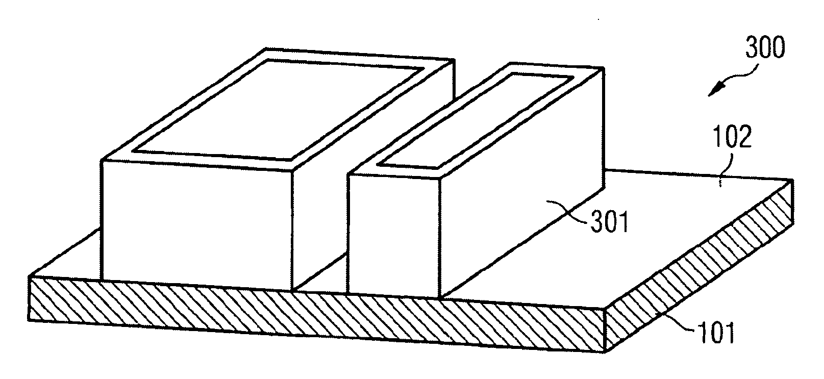
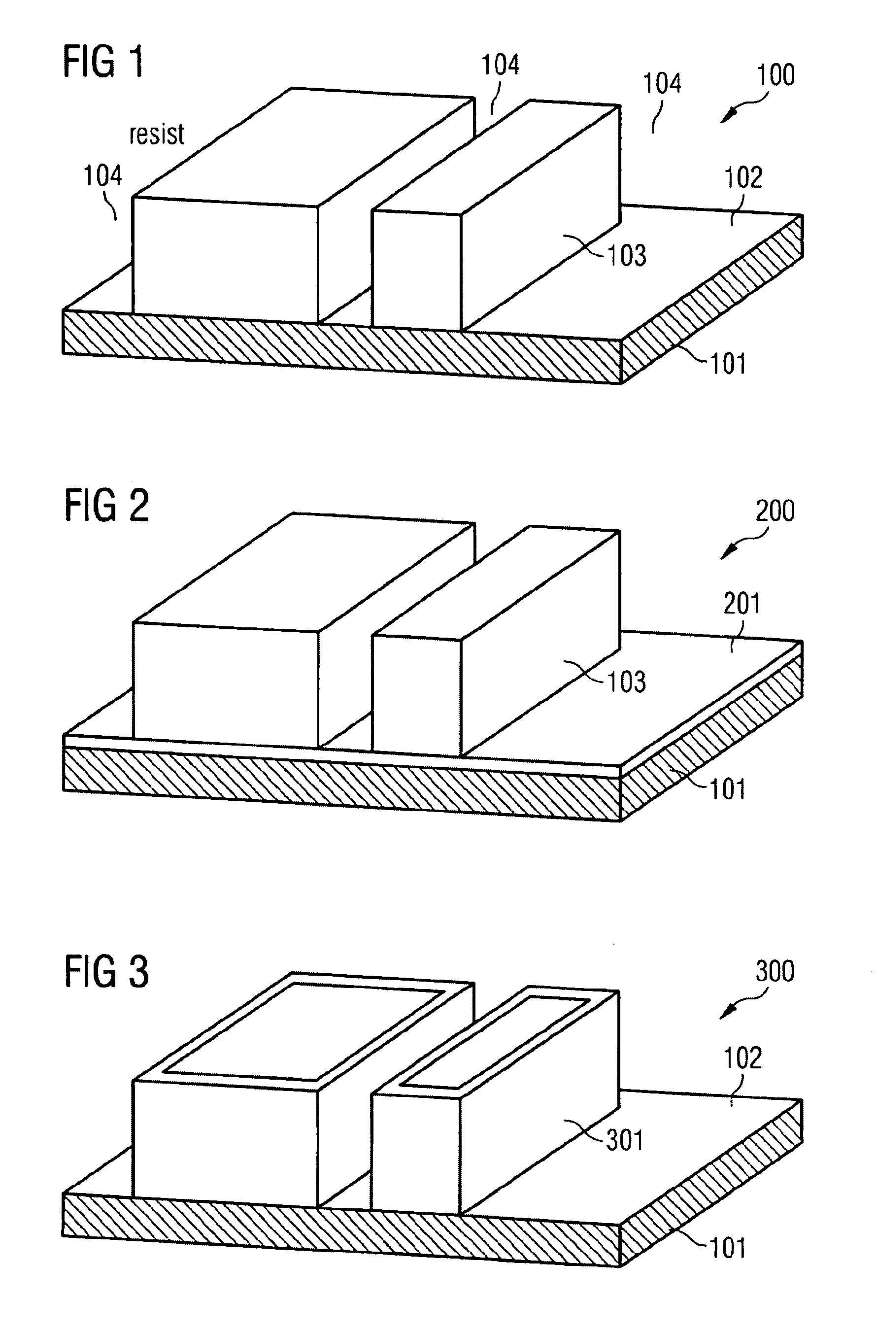
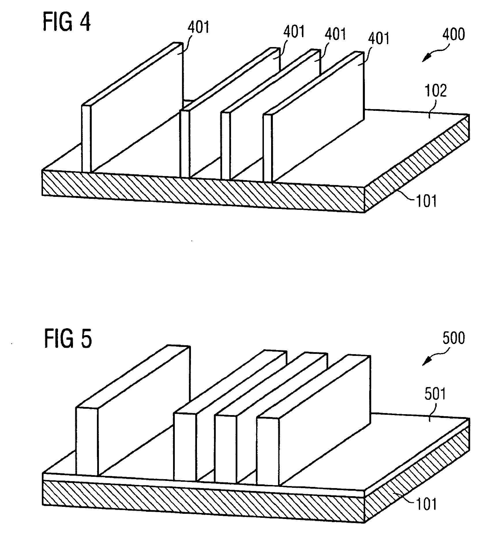
[0021] The invention may involve an application of a hard mask layer directly to the patterned photoresist layer using a low-temperature atomic layer epitaxy method. Horizontal regions of the hard mask layer are subsequently etched by an anisotropic etching process or technique. The hard mask layer may be considered “opened”, so that the patterned photoresist layer is at least partly uncovered in order subsequently to be removed. The vertical portions of the hard mask layer that have not been removed remain and have a layer thickness that can be set very precisely according to the dimensioning desired in the context of the atomic layer epitaxy method.

[0022] The present invention provides a cost-effective production process for forming sublithographic structures in a hard mask using customary mask types. On account of the use of an atomic layer epitaxy method for forming the hard mask layer, the thickness of the hard mask layer may be precisely controlled, and the hard mask layer is...


PUM


Abstract

An interconnect connection structure having first and second interconnects and multiple connection elements that electrically connect the first interconnect to the second interconnect is described. The multiple connection elements are formed laterally in a lateral region of the first and second interconnects relative to an overlay orientation of the interconnects. A central region may be free of connection elements so that electro-migration properties of the connection structure are improved and the current-carrying capacity is increased.

Description

PRIORITY AND CROSS REFERENCE TO RELATED APPLICATION [0001] This application is a continuation of International Application No. PCT / DE2004 / 002185, filed Sep. 30, 2004, which claims priority to German application 103 45 455.1, filed Sep. 30, 2003, both of which are incorporated in their entirety by reference herein.BACKGROUND OF THE INVENTION [0002] 1. Field of the Invention [0003] The invention relates hard masks, and particularly to methods for producing a hard mask and hard mask arrangements. [0004] 2. Description of the Related Art [0005] Optical lithography is used to produce feature sizes that are smaller than 100 nm. The chemistry used for a photoresist material, the production of mask(s) used in the optical lithography techniques and the complexity of the lithography tool used may be cost-intensive at these reduced feature sizes. The production of feature sizes smaller than 100 nm (“sub-100 nm structures”) has led to the development of optical lithography methods using light h...

Claims


Application Information

Patent Timeline
IPC IPC(8): G03F1/00H01L21/311H01L21/033
CPCH01L21/0338H01L21/0337
Inventor FEHLHABER, RODGERTEWS, HELMUT
Owner FEHLHABER RODGER
Learn More