Organic electroluminescence device
a technology of electroluminescence device and electroluminescence device, which is applied in the direction of discharge tube luminescnet screen, discharge tube/lamp details, coating, etc., can solve the problems of low work function metal activity and aptness, high film-forming temperature of materials, and relatively large poisonousness of materials, etc., to achieve high device luminance and efficiency, high device life, and high efficiency of electron injection
- Summary
- Abstract
- Description
- Claims
- Application Information
AI Technical Summary
Benefits of technology
Problems solved by technology
Method used
Image
Examples
embodiment 1
[0050] (1) Device structure:
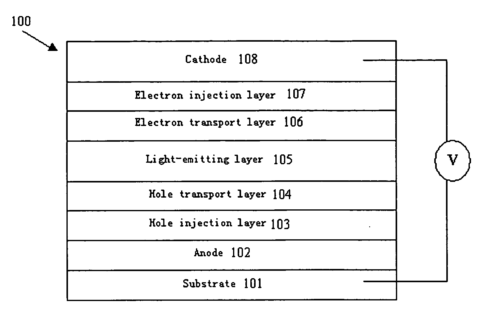
[0051] ITO / MTDATA(30 nm) / NPB(30 nm) / Alq3(55 nm) / Li3N(0.8 nm) / AI(150 nm)
[0052] (2) Preparation of an organic layer:
[0053] The preprocessed glass substrate is placed in a vacuum chamber which is pumped to 1×10⁻³ Pa. A MTDATA film of 30 nm is evaporated at an evaporation rate of 0.1 nm / s. Then, a layer of hole transport material NPB of 30 nm is evaporated on above film at an evaporation rate of 0.1 nm / s. On the hole transport layer, Alq3 of 55 nm is evaporated for a light-emitting layer and an electron transport layer of the device.
[0054] Wherein the glass substrate is comprised of an ITO (Indium Tin Oxide) film and a substrate. The Sheet Resistance of the ITO film is 50Ω, and its thickness is 150 nm.
[0055] (3) Preparation of an electron injection layer:
[0056] After evaporating the electron transport layer, Li3N of 0.8 nm is evaporated at an evaporation rate of 0.008 nm / s under temperature of 350° C. for an electron injection layer of the device.
[0057...
embodiment 2
[0060] (1) Device structure:
[0061] ITO / MTDATA(30 nm) / NPB(30 nm) / Alq3(55 nm) / K3N(1.5 nm) / Al(150 nm)
[0062] (2) Preparation steps are the same with Embodiment 1 except after evaporating the electron transport layer, K3N of 1.5 nm is evaporated.
embodiment 3
[0063] (1) Device structure:
[0064] ITO / MTDATA(30 nm) / NPB(30 nm) / Alq3(55 nm) / Cs3N(2.0 nm) / Al(150 nm)
[0065] (2) Preparation steps are the same with Embodiment 1 except after evaporating the electron transport layer, Cs3N of 2.0 nm is evaporated.
PUM
 Abstract
Description
Claims
Application Information
 - R&D
- Intellectual Property
- Life Sciences
- Materials
- Tech Scout
- Unparalleled Data Quality
- Higher Quality Content
- 60% Fewer Hallucinations
Browse by: Latest US Patents, China's latest patents, Technical Efficacy Thesaurus, Application Domain, Technology Topic, Popular Technical Reports.
© 2025 PatSnap. All rights reserved.Legal|Privacy policy|Modern Slavery Act Transparency Statement|Sitemap|About US| Contact US: help@patsnap.com


