
Thin-film capacitor element and semiconductor device

Inactive Publication Date: 2006-09-28
FUJITSU LTD
View PDF0 Cites 17 Cited by
  • Summary
  • Abstract
  • Description
  • Claims
  • Application Information

AI Technical Summary

Benefits of technology

[0011] The present invention has been achieved in order to solve the above problems. It is an object of the present invention to provide a thin-film capacitor element that uses a substrate made of silicon or the like and ferroelectric to remarkably improve the dielectric constant of the ferroelectric and increase electric capacity, and to provide a semiconductor device.

Problems solved by technology

However, the ferroelectric having such structures has an inconvenience in that dielectric characteristics such as a dielectric constant and a dielectric loss decrease as compared with those of the ferroelectric in a bulk state.
Therefore, the number of manufacturing steps increases, and this makes the manufacturing complex and decreases productivity.

Method used


Image

  • Thin-film capacitor element and semiconductor device
  • Thin-film capacitor element and semiconductor device
  • Thin-film capacitor element and semiconductor device

Examples


embodiments

[0043] The present invention will be explained in further detail below based on several embodiments.

first embodiment

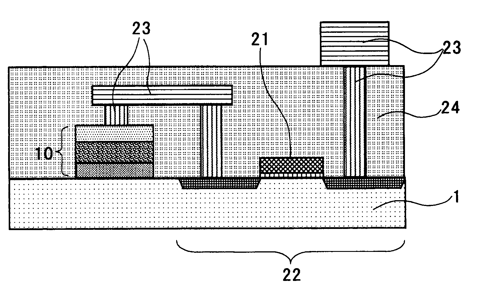
[0044]FIG. 3 is a diagram showing a thin-film capacitor according to a first embodiment of the present invention.

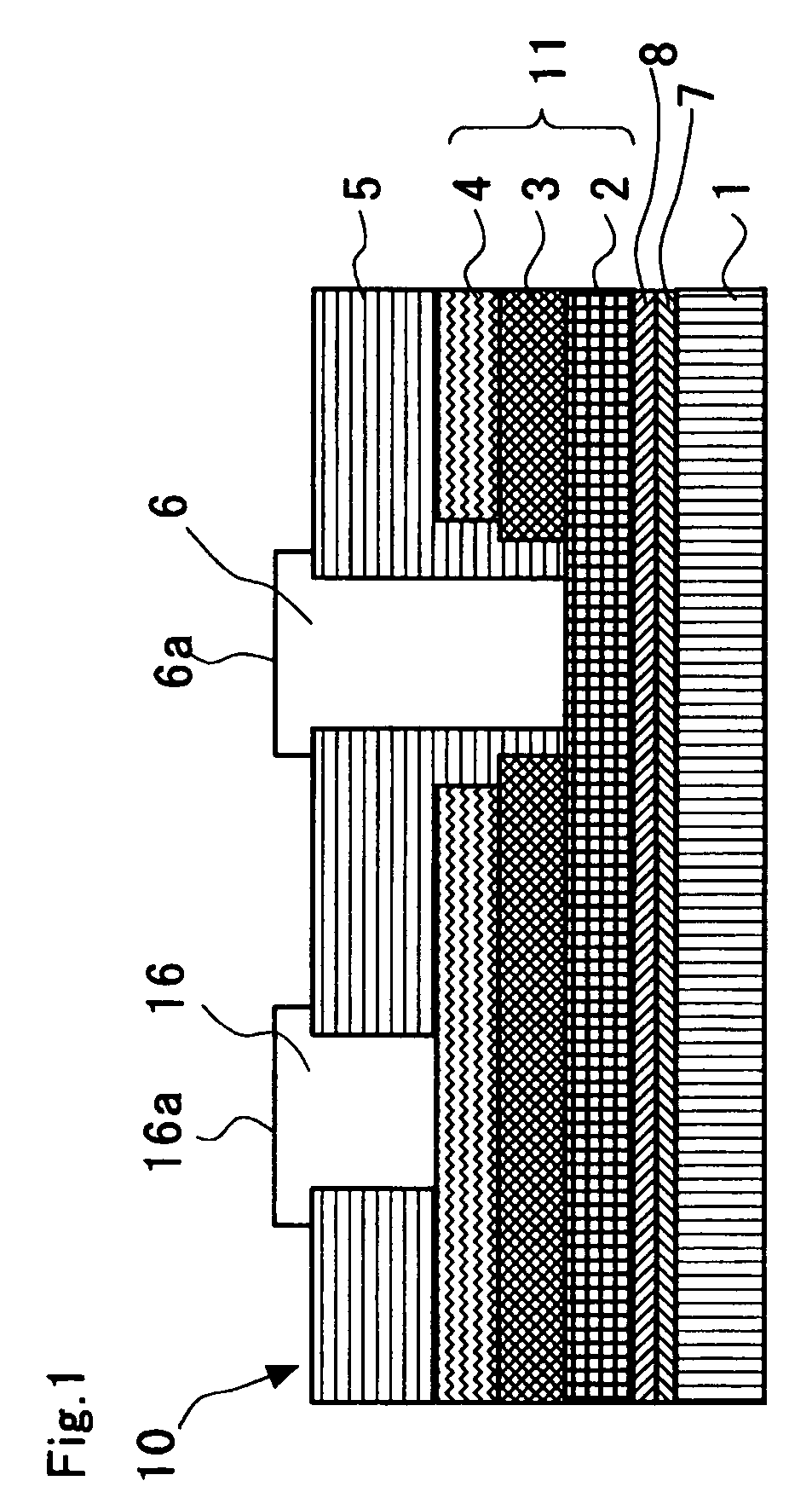
[0045] First, the adhesive layer 8 made of TiO2 having a film thickness of 20 nm is formed by the sputtering method via the insulating film 7 made of SiO2 that is obtained by thermal oxidation on the silicon substrate 1. Next, the lower electrode 2 made of Pt having a film thickness of 100 nm is formed by the sputtering method at a film forming temperature of 250° C. The ferroelectric layer 3 made of a high dielectric material Ba0.7Sr0.3TiO3 (BST) having a film thickness of 100 nm is formed by the sputtering method at a film forming temperature of 500° C. As a result, a BST / Pt / TiO2 / SiO2 / Si structure is obtained.

[0046] When a wafer curvature is measured at this stage, the BST / Pt / TiO2 / SiO2 / Si structure has a tensile stress of +408.2 MPa.

[0047] In order to compensate for the tensile stress, an IrO2 film having a compressive stress within a range from 500 MPa to 5 GPa is f...

second embodiment

[0049]FIG. 4 is a diagram showing a thin-film capacitor according to a second embodiment of the present invention.

[0050] In the second embodiment, a metal layer 9 of gold (Au) is formed on the upper electrode 4 of the thin-film capacitor having the IrO2 / BST / Pt / TiO2 / SiO2 / Si structure manufactured in the first embodiment. When a wafer curvature of this thin-film capacitor is measured at this stage, this capacitor has a compressive stress of −787 MPa.

[0051] When the metal layer 9 of gold (Au) is formed, the dielectric constant can be further increased from that of the capacitor element having the structure according to the first embodiment.

[0052] As explained above, when the compressive stress of at least one of the conductive electrodes of the capacitor element according to the present invention is 10 MPa to 5 GPa, preferably 100 MPa to 5 GPa, the tensile stress of silicon or the like can be compensated for, thereby significantly increasing the dielectric constant.

[0053]FIG. 5 is ...


PUM


Abstract

A thin-film capacitor element has at least a lower electrode, a ferroelectric layer, and an upper electrode. The upper electrode adds a compressive stress of 10 MPa to 5 GPa to the ferroelectric layer. The upper electrode includes at least one oxide selected from PtOx, IrOx, RuOx, SrRuOy, and LaNiOy.

Description

CROSS-REFERENCE TO RELATED APPLICATIONS [0001] This application is based upon and claims the benefit of priority from the prior Japanese Patent Application No. 2005-91845, filed on Mar. 28, 2005, the entire contents of which are incorporated herein by reference. BACKGROUND OF THE INVENTION [0002] 1) Field of the Invention [0003] The present invention relates to a thin-film capacitor element having a capacitor structure formed on a substrate such as a semiconductor substrate by a thin-film manufacturing process, and to a semiconductor device. [0004] 2) Description of the Related Art [0005] In recent years, application of a thin-film capacitor element made of a high dielectric constant oxide and ferroelectric oxide is considered as a decoupling capacitor that suppresses voltage noise and a voltage variation in a power bus line, a storage capacitor in a dynamic random access memory (DRAM) and a ferroelectric random access memory (FRAM), and a tunable capacitor in a microwave device. Pa...

Claims


Application Information

Patent Timeline
IPC IPC(8): H01L29/76
CPCH01G4/005H01G4/33H01G7/06H01L27/1085H01L27/11502H01L27/11507H01L28/55H01L28/65H10B12/03H10B53/30H10B53/00
Inventor BARIECKI, JOHN DAVIDSHIOGA, TAKESHIKURIHARA, KAZUAKI
Owner FUJITSU LTD
Learn More