Lithography mask and methods for producing a lithography mask

Inactive Publication Date: 2006-09-21
QIMONDA
View PDF6 Cites 2 Cited by
  • Summary
  • Abstract
  • Description
  • Claims
  • Application Information

AI Technical Summary

Benefits of technology

[0014] In this case, an alternating arrangement means, in particular, that in the case of a linear dense arrangement of structures, the latter are produced alternately by second and third regions of the lithography mask. In the case of an areal dense arrangement of structures, second and third regions are arranged alternately in each case in two directions that are essentially perpendicular to one another, similarly to the black and white areas on a chessboard, but spaced apart from one another. The alternating or alternative arrangement of second and third regions has the effect that generally a third region is arranged closest adjacent to each second region and a second region is arranged closest adjacent to each third region. Within the altPSM section, preferably each second and each third region is singly contiguous.
[0016] The invention has an advantage that even when there is a relative lateral offset between the first and second resist masks, which offset can be avoided with a disproportionate outlay in practice, no residues of the nontransparent layer remain between second and third regions which are intended to adjoin one another. This is of particular importance in the case of lithography masks having the abovementioned RIM structures in which a third region is arranged within a multiply contiguous second region. Therefore, the invention is particularly suitable for the above-described lithography mask having altPSM sections and RIM sections. A further advantage of this invention is that the second resist mask can be produced with a lower lateral resolution. The tolerance range with regard to a relative lateral offset between the two resist masks and with regard to the lateral resolution is determined by the width of the peripheral edge region of the third region which is not covered by the second resist mask.

Problems solved by technology

The technologies of the documents mentioned have specific disadvantages, in particular for example restrictions with regard to the process window or the permissible parameter ranges during the lithographic imaging of the lithography mask.
A general and fundamental problem is furthermore the fabrication of lithography masks with the required precision, in particular for example with the required relative positional accuracy of nontransparent and transparent regions.

Method used


Image

  • Lithography mask and methods for producing a lithography mask
  • Lithography mask and methods for producing a lithography mask
  • Lithography mask and methods for producing a lithography mask

Examples


Embodiment Construction

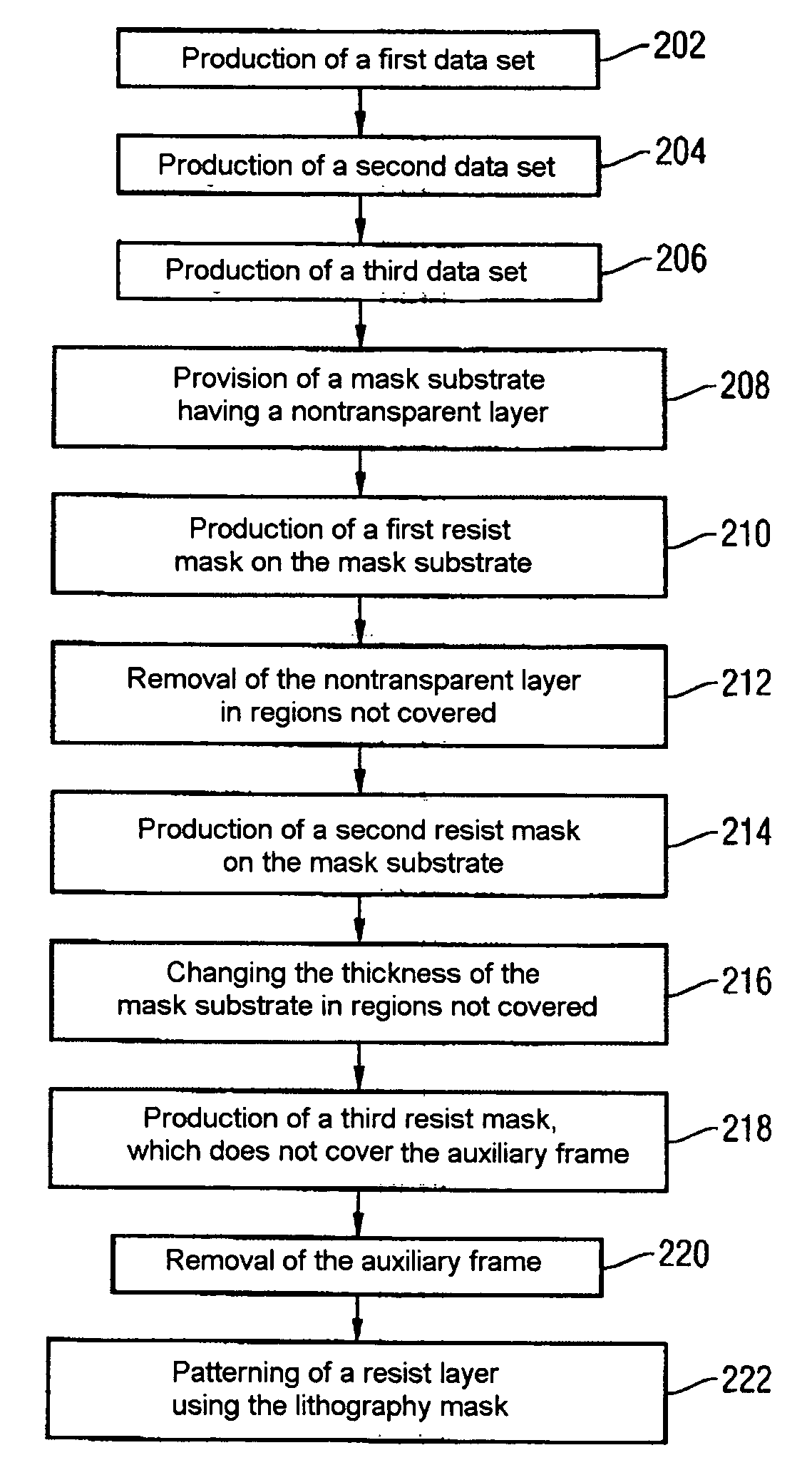
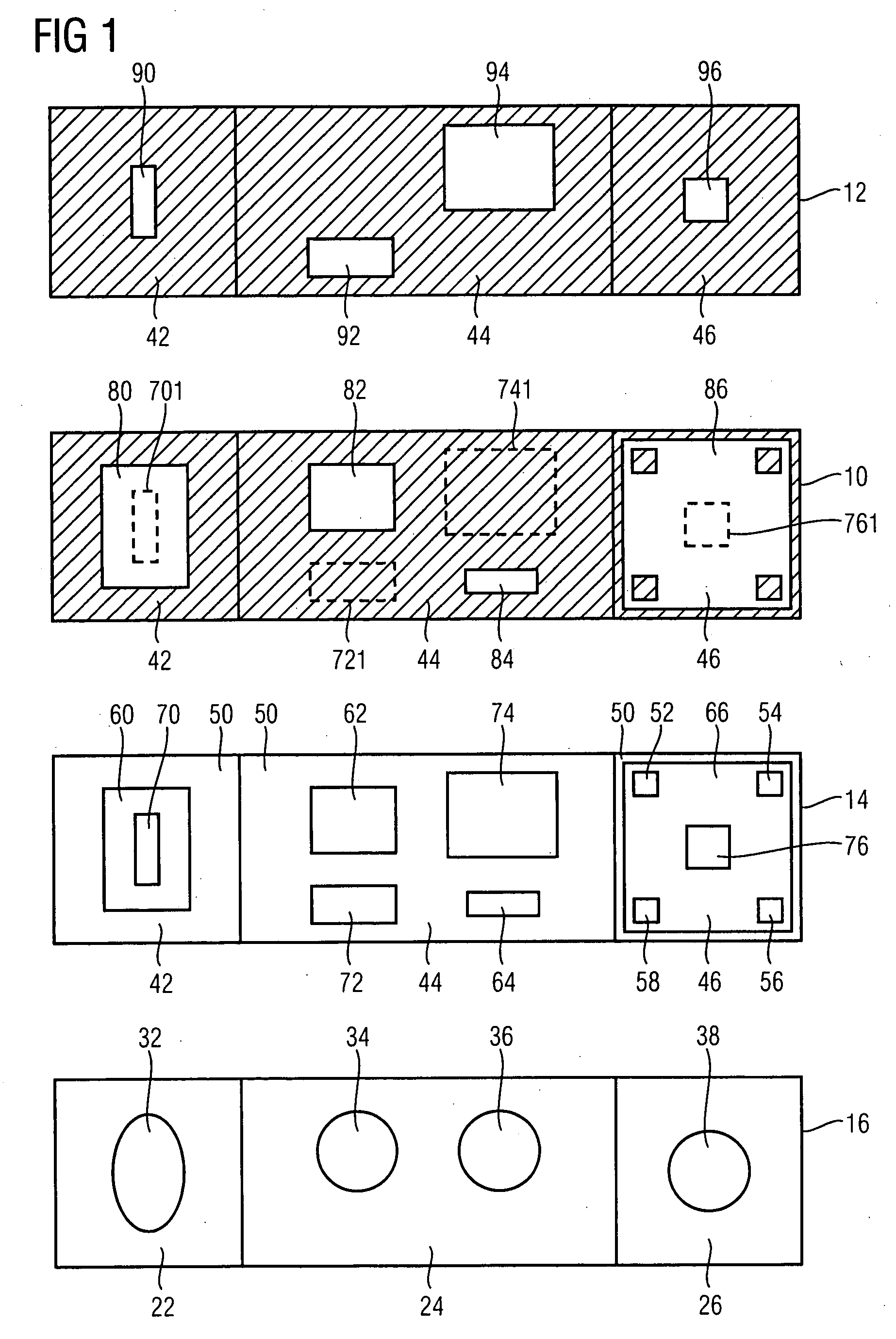
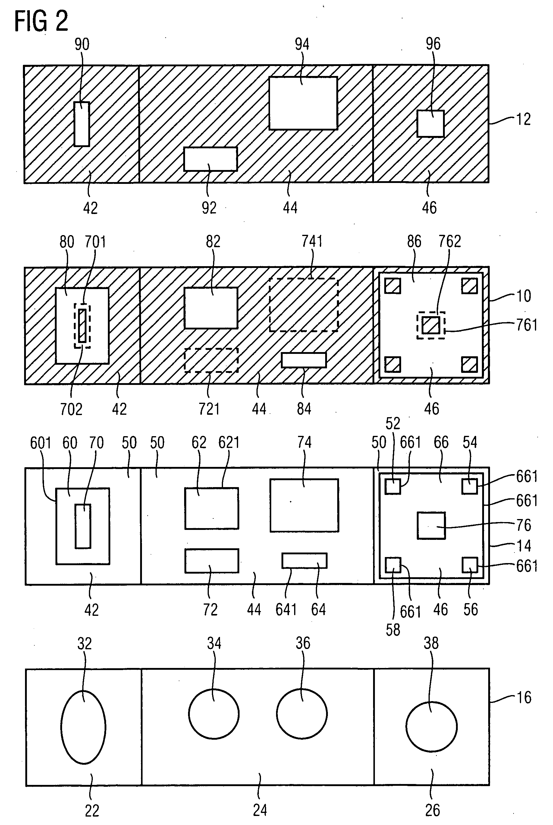
[0024]FIG. 1 is a schematic illustration of a first exemplary embodiment of the present invention. It shows schematic plan views of a first resist mask 10, a second resist mask 12, a finished lithography mask 14 fabricated by means of the resist masks 10, 12, and a substrate 16 patterned lithographically by means of the lithography mask 14. The resist masks 10, 12 are produced during the fabrication of the lithography mask 14 on the mask substrate thereof. Afterward, their lateral structures, as described below, are transferred into or onto the mask substrate in order to obtain the lithography mask 14.

[0025] The patterned substrate 16 has a first section 22, a second section 24 and a third section 26 each having one or a plurality of contact holes or passage holes 32, 34, 36, 38. The passage holes 32, 34, 36, 38 penetrate through the visible topmost layer of the patterned substrate 16 in order, by way of example, to produce electrically conductive connections between wiring planes ...


PUM


Abstract

Lithography mask for the lithographic patterning of a resist layer on a substrate having first regions, in which the lithography mask has a nontransparent layer, and second and third regions, which differ in terms of the optical thickness of the lithography mask and in which the lithography mask is at least semitransparent. The lithography mask comprises a first section having a plurality of second regions and a plurality of third regions, which are arranged alternately and surrounded by a first region, for the lithographic production of resist openings at distances which are less than a predetermined limit distance. Furthermore, the lithography mask comprises a second section having a multiplicity of third regions, each of which is surrounded by a second region surrounded by a multiply contiguous first region, for the lithographic production of resist openings at distances which are greater than a predetermined limit distance.

Description

CLAIM FOR PRIORITY [0001] This application claims the benefit of priority to German Application No. 10 2005 009 805.3, filed in the German language on Mar. 3, 2005, the contents of which are hereby incorporated by reference. TECHNICAL FIELD OF THE INVENTION [0002] The present invention relates to a lithography mask for the lithographic production of dense and isolated contact holes, and to methods which are particularly suitable for producing such a lithography mask. BACKGROUND OF THE INVENTION [0003] In microelectronic or micromechanical components, structures at small distances from one another, in particular at distances which are less than the wavelength used for their lithographic production, are referred to as dense structures. Structures at larger distances from one another are referred to as semi-isolated or isolated structures. In the fabrication of a microelectronic or micromechanical component, a minimum number of process steps is advantageous inter alia for cost reasons....

Claims


Application Information

Patent Timeline
IPC IPC(8): G03C5/00G03F1/00
CPCG03F1/144G03F1/32G03F1/29G03F1/38G03F1/36
Inventor HENKEL, THOMASKOHLE, RODERICKNOLSCHER, CHRISTOPHRENNER, KERSTIN
Owner QIMONDA
Why Eureka
Try Eureka