
Comparator-based switched capacitor circuit for scaled semiconductor fabrication processes

a switched capacitor and fabrication process technology, applied in the field of switching capacitor circuits, can solve the problems of low power, high speed digital, high power, and low performance of analog circuits

Active Publication Date: 2006-09-21
MASSACHUSETTS INST OF TECH
View PDF3 Cites 18 Cited by
  • Summary
  • Abstract
  • Description
  • Claims
  • Application Information

AI Technical Summary

Benefits of technology

The invention features a switched capacitor circuit for performing analog circuit functions. The circuit includes a comparator and a load capacitor, and a method for sampling an input voltage and applying reference voltages to the circuit during different phases. The circuit can also include a clocked comparator and sampling capacitors with different terminals for receiving the input voltage and reference voltages. The technical effects of the invention include improved accuracy and efficiency in analog circuit functions and reduced noise in the signal-to-noise ratio.

Problems solved by technology

Process advancements such as lower voltage power supplies and shorter gate lengths result in low power, high speed digital circuits, but can also result in higher power, low performance analog circuits.
Lower output resistance, reduced power supply voltage, increased threshold variation and gate leakage present design challenges for analog and mixed signal systems.
The design of high gain operational amplifiers (hereafter op-amps) is one example of a design challenge resulting from the continued scaling of CMOS processes.
Moreover, it is not practical to maintain an acceptable intrinsic gain per unit current by using longer devices in a scaled implementation, especially when increased frequency capability is required.
In addition, the output resistance of modem scaled devices is not linearly proportional to gate length; increasing the gate length does not significantly increase the output resistance of the device.
To achieve satisfactory gain in an amplifier designed in a scaled process, it is often necessary to utilize a cascode topology; however, a cascode topology using a reduced supply voltage generally results in a substantially reduced voltage swing.
In a highly scaled CMOS process it is generally difficult to achieve the required op-amp performance.

Method used


Image

  • Comparator-based switched capacitor circuit for scaled semiconductor fabrication processes
  • Comparator-based switched capacitor circuit for scaled semiconductor fabrication processes
  • Comparator-based switched capacitor circuit for scaled semiconductor fabrication processes

Examples


Embodiment Construction

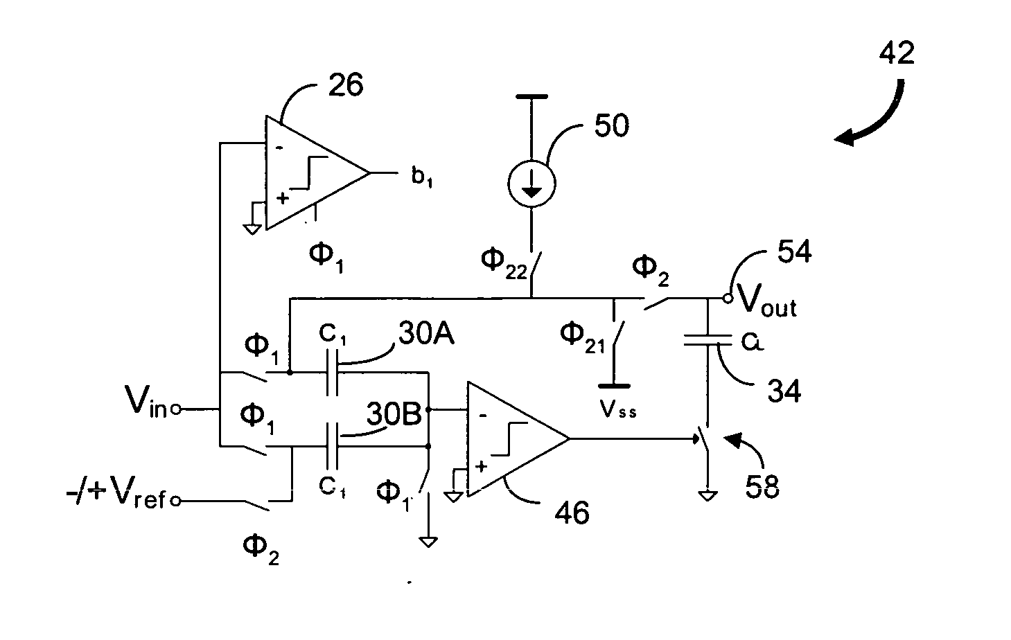
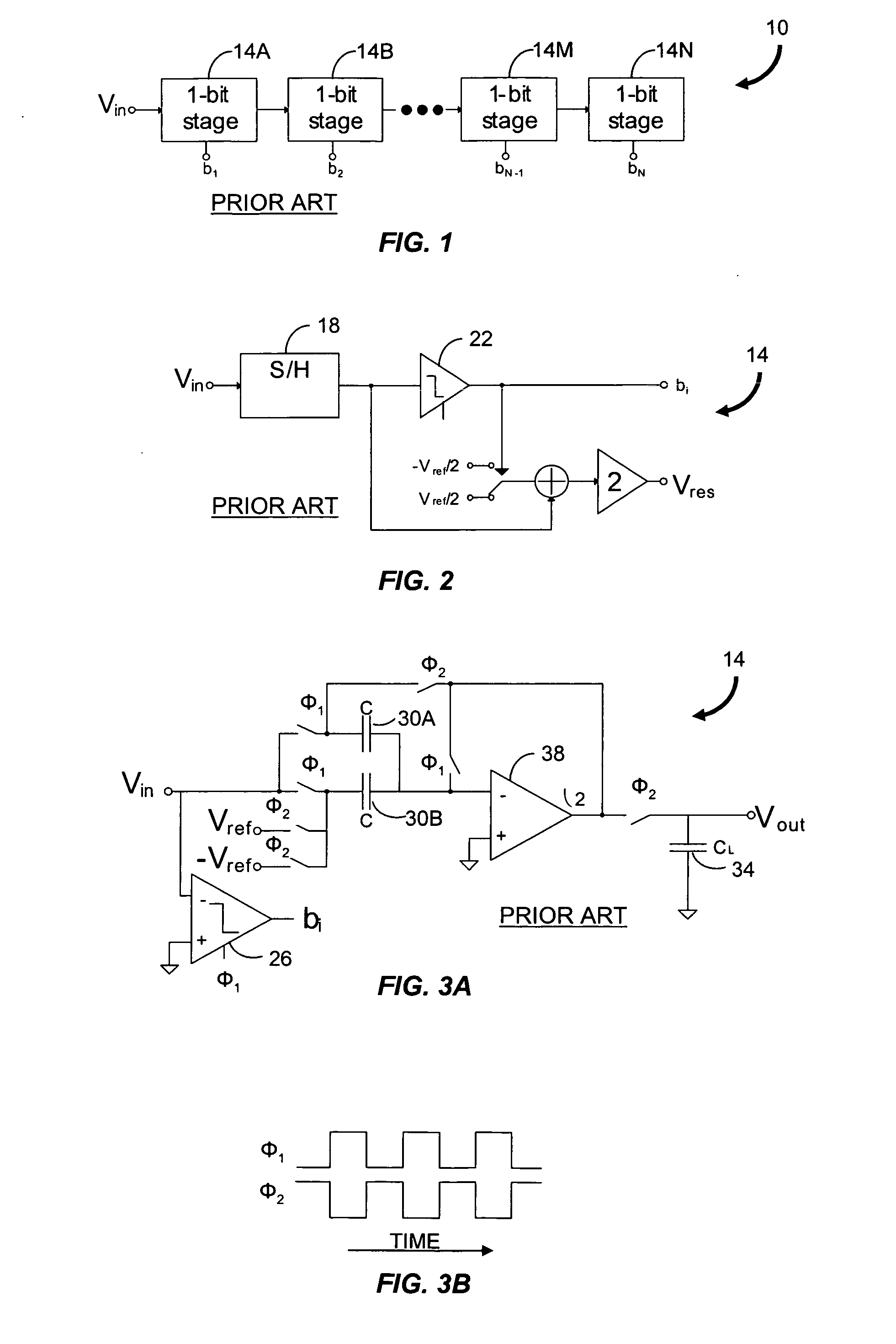
[0023] In brief overview, the present invention relates to a switched capacitor circuit having a comparator for high gain amplification in integrated circuits. Unlike conventional switched capacitor circuits employing op-amps, the switched capacitor circuit of the present invention uses a comparator and does not require direct feedback between the input and output of the comparator. Because feedback is eliminated, the design requirements of the switched capacitor circuit are relaxed and various scaled CMOS processes (e.g., 90 nm CMOS) can be used to fabricate the circuit. The circuit provides improved performance when compared with op-amp based switched capacitor circuits. Although the circuit is described below with respect to a pipeline analog-to-digital converter (ADC), the switched capacitor circuit of the present invention can be used with any of a variety of circuits based on switched capacitors, including generally ADCs, digital-to-analog converters (DACs), sample and hold ci...


PUM


Abstract

Described is a switched capacitor circuit for performing an analog circuit function. Unlike conventional switched capacitor circuits employing operational amplifiers, the switched capacitor circuit uses a comparator and does not require direct feedback between the input and output of the comparator. The switched capacitor circuit includes a first and a second switched capacitance network, a comparator and a current source. The first switched capacitance network has an input terminal to receive a circuit input voltage during a first phase. The comparator has an input terminal in communication with the first switched capacitance network and an output terminal in communication with the second switched capacitance network through a switched terminal. The current source communicates with the switched capacitance networks and supplies a current to charge the networks during a second phase. The circuit can be used, for example, to provide high gain amplification in integrated circuits.

Description

RELATED APPLICATION [0001] This application claims the benefit of the earlier filing date of U.S. Provisional Patent Application Ser. No. 60 / 663,850, filed Mar. 21, 2005, entitled “Switched Capacitor Circuits without Operational Amplifiers,” the entirety of which is incorporated herein by reference.FIELD OF THE INVENTION [0002] The present invention relates generally to a switched capacitor circuit and, more particularly, to a switched capacitor circuit for integrated circuits manufactured according to scaled semiconductor processes. BACKGROUND OF THE INVENTION [0003] Modern scaled complementary metal-oxide semiconductor (CMOS) processes are typically optimized for digital circuits. Process advancements such as lower voltage power supplies and shorter gate lengths result in low power, high speed digital circuits, but can also result in higher power, low performance analog circuits. Lower output resistance, reduced power supply voltage, increased threshold variation and gate leakage ...

Claims


Application Information

Patent Timeline
Patent Type & Authority Applications(United States)
IPC IPC(8): H03M1/12
CPCH03F3/005H03M1/38
Inventor FIORENZA, JOHN K.SEPKE, TODDLEE, HAE-SEUNGSODINI, CHARLES G.
Owner MASSACHUSETTS INST OF TECH
Learn More