Interconnecting substrate and semiconductor device

Active Publication Date: 2006-08-31
RENESAS ELECTRONICS CORP
View PDF6 Cites 49 Cited by
  • Summary
  • Abstract
  • Description
  • Claims
  • Application Information

AI Technical Summary

Benefits of technology

[0023] a warpage-controlling pattern which is provided in the sunken section in the bottom surface of the base insulating film and is formed in such a manner as to suppress a warpage of the interconnecting substrate toward a bottom side on both sides of the first direction.
[0036] According to the present invention, it is possible to provide an interconnecting substrate which has sufficient mechanical strength but in which warpage is controlled. As a result, the transferability in the semiconductor chip-mounting step is improved and productivity can be improved. At the same time, a semiconductor device having high reliability can be provided.

Problems solved by technology

However, this builtup printed substrate has the problem that because of the use of a glass epoxy printed substrate of low heat resistance as the base core substrate, deformation, such as shrinkage, warpage and waviness, is apt to occur due to the heating during the formation of a multilayer structure and the carrying of a semiconductor chip.
However, because in this interconnecting substrate for packaging, external electrode terminals 508 are formed by the etching of metal sheet 501, it is difficult to narrow the pitch between external electrode terminals 508 due to limits to the control of the quantity of side etching during etching.
Furthermore, when this interconnecting substrate for packaging is mounted on an external board and a device, structurally, stresses are concentrated on the interface between external electrode terminal 508 and insulating layer 502, thereby posing the problem that open faults tend to occur and hence sufficient reliability cannot be obtained.
However, an interconnecting substrate having a structure as described in Patent Document 2 had the problem that a warpage occurs after manufacture although it is excellent in heat resistance and mechanical strength according to the characteristics of an insulating material.
On that occasion, the warpage of the block substrate lowers transfer efficiency, and makes it difficult to perform precise mounting of semiconductor chips, thereby causing a decrease in throughput, yield and connection reliability.

Method used


Image

  • Interconnecting substrate and semiconductor device
  • Interconnecting substrate and semiconductor device
  • Interconnecting substrate and semiconductor device

Examples


Embodiment Construction

[0049] Hereinafter, preferred embodiments of the present invention will be described.

Basic Structure of Interconnecting Substrate

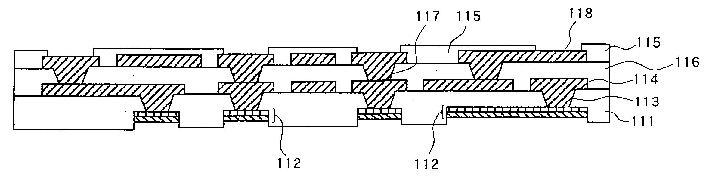
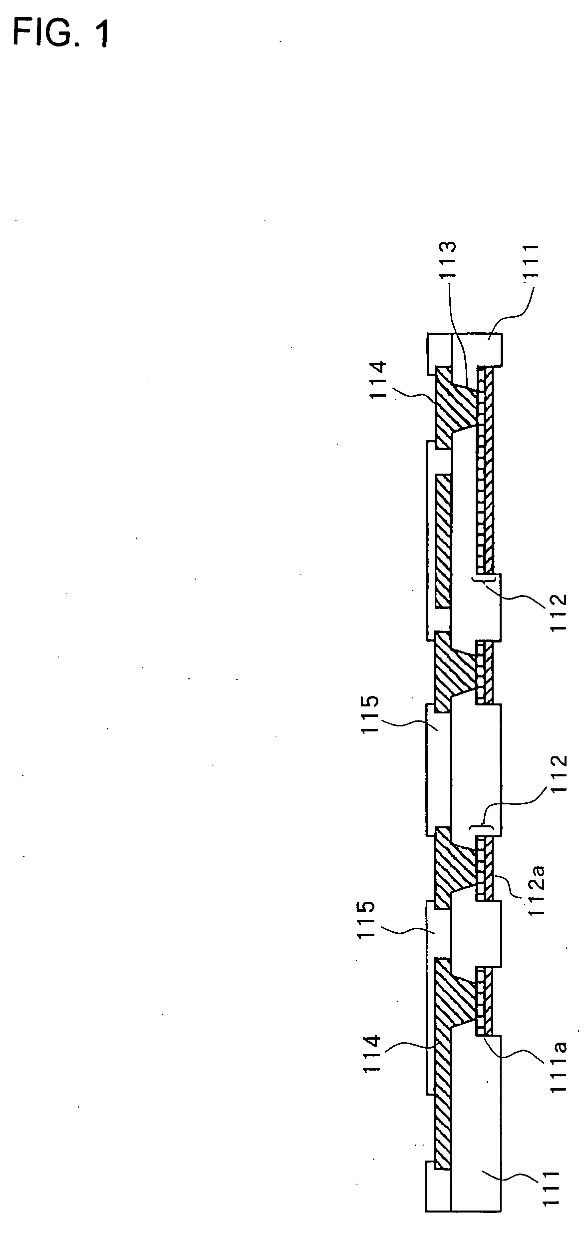
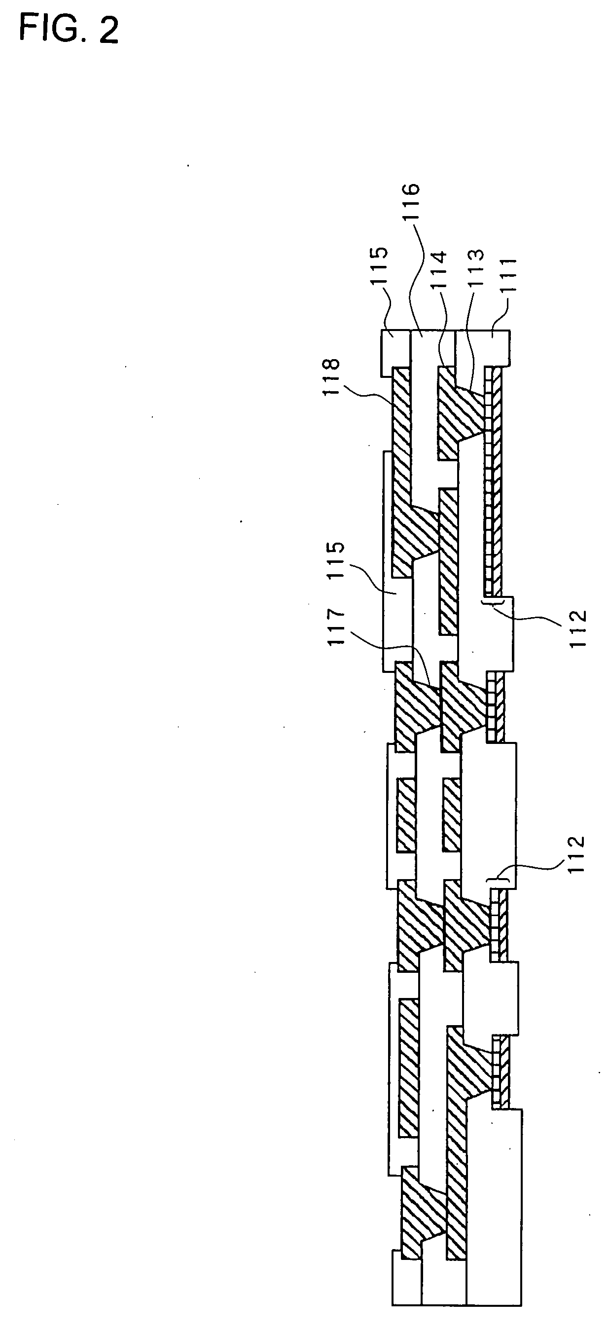
[0050] First, a basic structure of an interconnecting substrate of the present invention will be described by using an embodiment shown in FIG. 1.

[0051] An interconnecting substrate of the present embodiment has base insulating film 111, lower layer interconnection 112 provided on a bottom surface side of this base insulating film, via hole 113 formed in the base insulating film, and upper layer interconnection 114 which is connected to the lower layer interconnection via a conductor within this via hole and is formed on a top surface of the base insulating film. Lower layer interconnection 112 is provided within sunken section 111a of a bottom surface of base insulating film 111. On base insulating film 111, solder resist layer 115 is formed in such a manner as to cause part of upper layer interconnection 114 to be exposed and cover a remaining part t...


PUM


Abstract

An interconnecting substrate is provided with a base insulating film having a sunken section in a bottom surface thereof, a first interconnection provided in the sunken section, a via hole formed in the base insulating film, and a second interconnection which is connected to the first interconnection via a conductor within the via hole and is formed on a top surface of the base insulating film, wherein the interconnecting substrate comprises a first interconnection pattern formed of the first interconnection which comprises at least a linear pattern which extends along a second direction orthogonal to a first direction, and a warpage-controlling pattern which is provided in the sunken section in the bottom surface of the base insulating film and is formed in such a manner as to suppress a warpage of the interconnecting substrate toward a bottom side on both sides of the first direction.

Description

BACKGROUND OF THE INVENTION [0001] 1. Field of the Invention [0002] The present invention relates to an interconnecting substrate used for carrying a semiconductor chip and a semiconductor device in which this interconnecting substrate is used. [0003] 2. Description of the Related Art [0004] In recent years, as a result of an increase in the number of terminals and a narrower pitch due to the high performance design, multifunctional design and high density design of semiconductor devices, interconnecting substrates for packaging on which semiconductor devices are to be mounted have been required to provide high density and fine pitch design more than before. [0005] A build-up printed substrate, which is a type of a multilayer interconnecting substrate, has hitherto been-mentioned as an interconnecting substrate for packaging which is widely used. In this builtup printed substrate, resin layers are formed on both surfaces of a glass epoxy printed substrate as a base core substrate, o...

Claims


Application Information

Patent Timeline
IPC IPC(8): H01L23/52
CPCH01L21/6835H01L2224/16235H01L23/49822H01L23/49827H01L23/49838H01L25/0657H01L2221/68345H01L2224/16H01L2224/83102H01L2224/92125H01L2225/06517H01L2225/06541H01L2225/06572H01L2924/01046H01L2924/01078H01L2924/01079H01L2924/09701H01L2924/15311H01L2924/1532H01L2924/3511H05K1/113H05K3/107H05K3/205H05K3/4682H05K2201/09472H05K2201/096H05K2203/0384H01L2924/01019H01L23/49816H01L2924/10253H01L2224/73204H01L2224/32225H01L2224/16225H01L2924/00H01L2224/16237H01L2924/00014H01L2924/00011H01L2224/0401G06Q50/26G06Q10/04H04W84/18G08B31/00
Inventor OGAWA, KENTATSUKANO, JUNMAEDA, TAKEHIKOSHIMOTO, TADANORIYAMAMICHI, SHINTAROBABA, KAZUHIRO
Owner RENESAS ELECTRONICS CORP
Why Eureka
Try Eureka