Solution treatment apparatus and solution treatment method

a technology of solution treatment and treatment method, which is applied in the direction of liquid surface applicators, pretreated surfaces, coatings, etc., can solve the problem of large space requirements, and achieve the effect of increasing throughpu

Active Publication Date: 2006-08-24
TOKYO ELECTRON LTD
View PDF4 Cites 13 Cited by
  • Summary
  • Abstract
  • Description
  • Claims
  • Application Information

AI Technical Summary

Benefits of technology

[0009] The present inventors study separating a block including the coating unit of the resist solution being a solution treatment unit for forming a resist film and a forming unit of an anti-reflection film from a block in which developing treatment is performed, and independently forming a

Problems solved by technology

Since the exhaust pipes have a large diameter, a large space is required when the exh

Method used


Image

  • Solution treatment apparatus and solution treatment method
  • Solution treatment apparatus and solution treatment method
  • Solution treatment apparatus and solution treatment method

Examples


Embodiment Construction

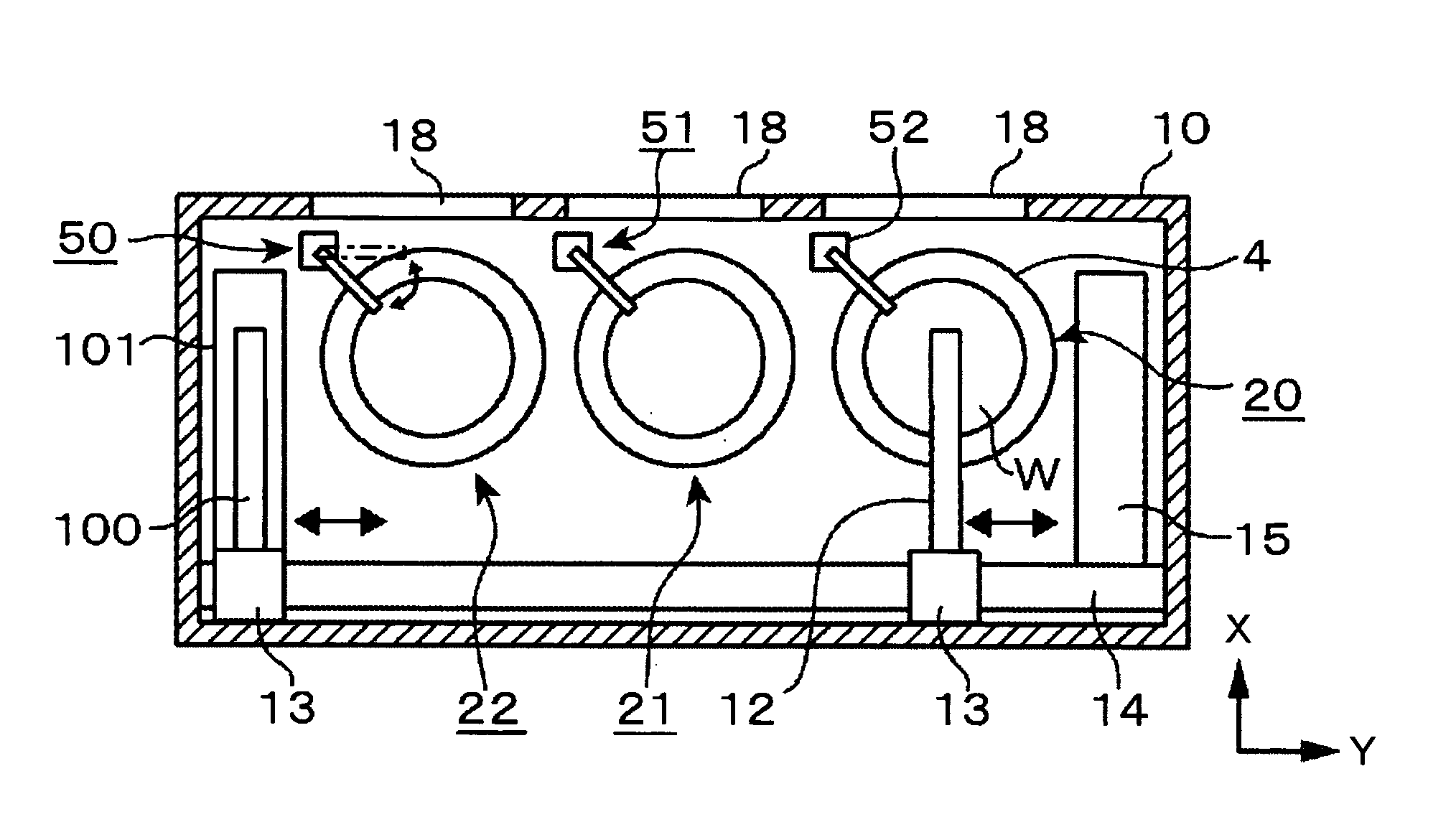
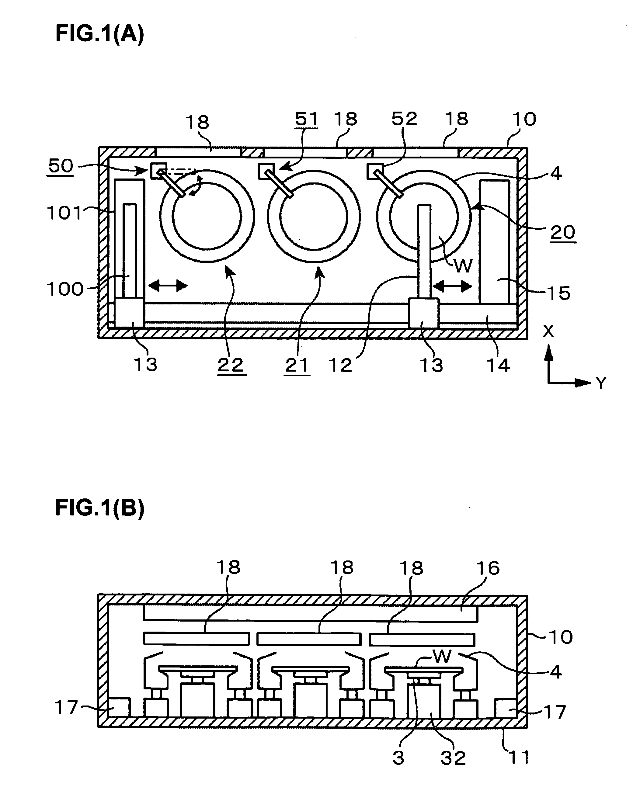
[0035] An embodiment in which a solution treatment apparatus according to the present invention is applied to a coating apparatus of a resist solution will be described. In FIGS. 1A and 1B, a numeral 10 denotes a solution treatment apparatus in which three solution treatment sections 20, 21, and 22 are provided in a common casing 11 such that they are arranged in a horizontal direction (Y-axis direction) in this example. These solution treatment sections 20, 21, and 22 have the same configuration and therefore will be described in detail with reference to FIG. 2 taking the solution treatment section 20 as an example.

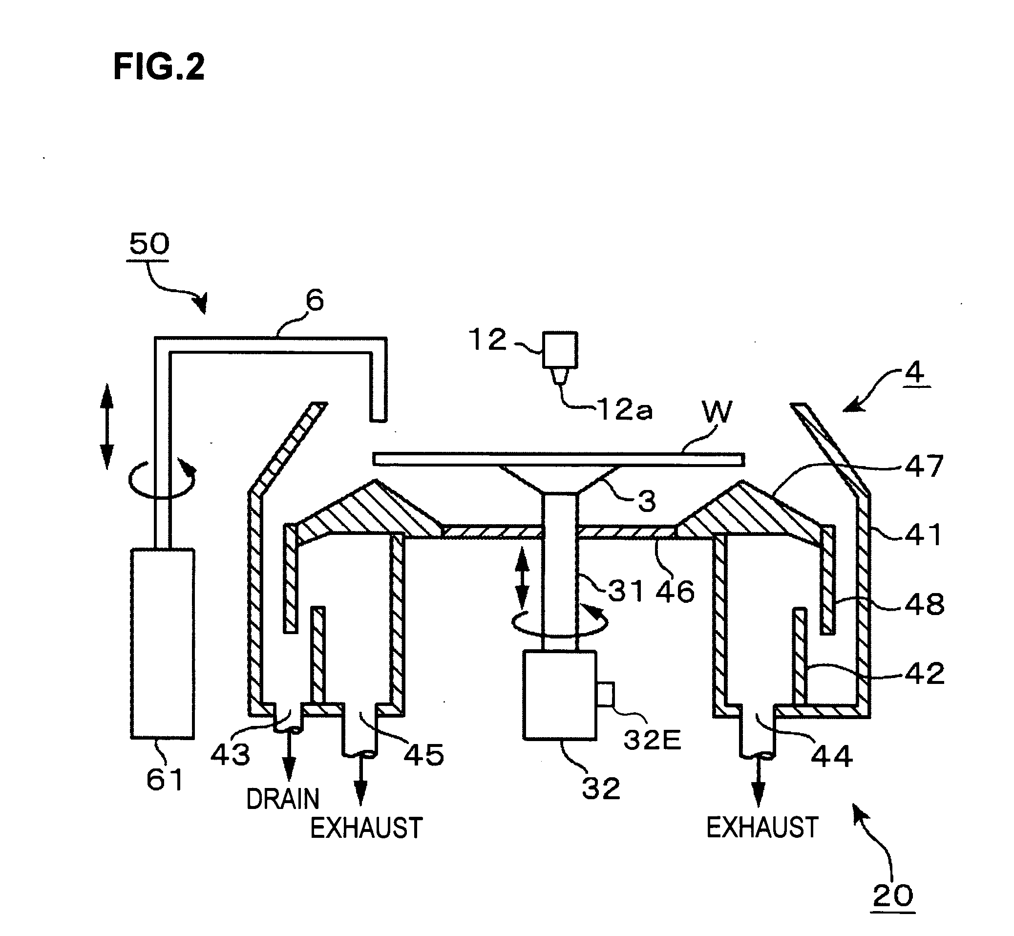
[0036] In FIG. 2, a numeral 3 denotes a spin chuck being a substrate holding portion for horizontally holding a wafer W by absorbing by suction the central portion on the rear face side of the wafer W. The spin chuck 3 is connected via a shaft portion 31 to a drive mechanism (spin chuck motor) 32 and configured to be capable of rotating and rising and lowering while hol...


PUM


Abstract

In the present invention, a plurality of exhaust paths connected to a plurality of cup bodies surrounding substrate holding portions respectively are joined together for common use, and the openings of exhaust rate adjustment sections provided on the exhaust paths are adjusted with reference to data in which combinations of the numbers of rotations of the substrate holding portions are associated with combinations of set exhaust rates of the exhaust paths when solution treatment is performed by rotating the substrate by the substrate holding portion. According to the present invention, the cup body can be exhausted at an intended exhaust rate at all times independently of the state where the substrate in which cup body is subjected to which process.

Description

BACKGROUND OF THE INVENTION [0001] 1. Field of the Invention [0002] The present invention relates to a solution treatment apparatus for performing solution treatment, for example, application of a resist, developing treatment after exposure, or the like, for a substrate such as, for example, a semiconductor wafer or a glass substrate for a liquid crystal display (LCD substrate), and a method therefor. [0003] 2. Description of the Related Art [0004] The process of forming a resist pattern on a substrate that is one of manufacturing processes of a semiconductor device or an LCD substrate is performed by a series of processes of forming a resist film on the substrate, for example, a semiconductor wafer (hereinafter, referred to as a wafer), exposing the resist film to light using a photomask, and thereafter performing developing treatment so as to obtain a desired pattern. The series of processes have conventionally been performed by a coating and developing apparatus. [0005] The coati...

Claims


Application Information

Patent Timeline
IPC IPC(8): H01L21/20
CPCH01L21/6715H01L21/67178H01L21/67253B01L9/06B01L9/04B01L2200/02
Inventor MATSUOKA, NOBUAKINAKASHIMA, TSUNENAGAHAYASHI, SHINICHIOOZONO, AKIRA
Owner TOKYO ELECTRON LTD
Why Eureka
Try Eureka