
Magnetoresistive effect element, magentic memory device and manufacturing method of magnetoresistive effect element and magnetic memory device

a technology of magnetic memory device and effect element, which is applied in the field of magnetic memory device and manufacturing method of magnetoresistive effect element and magnetic memory device, can solve the problems of slow information writing speed, inability to write so many times, and difficulty in selectively writing information using asteroid characteristics, so as to improve the effect of coercive force fluctuations and improve the rectangle property of resistance-external magnetic field curv

Inactive Publication Date: 2006-08-24
SONY CORP
View PDF3 Cites 37 Cited by
  • Summary
  • Abstract
  • Description
  • Claims
  • Application Information

AI Technical Summary

Benefits of technology

This approach results in improved magnetic characteristics, reducing write errors and allowing for stable and selective information writing in magnetic memory devices by controlling magnetic anisotropies and coercive force fluctuations.

Problems solved by technology

However, flash memories have a defect that the information writing speed thereof is slow as the order of microseconds.
On the other hand, it has been pointed out that the FRAM cannot be rewritten so many times.
In the MRAM, when magnetic characteristics of the TMR elements fluctuate at every element or magnetic characteristics fluctuate when the same element is repeatedly used, there arises a problem in which it becomes difficult to selectively write information by using the asteroid characteristics.

Method used


Image

  • Magnetoresistive effect element, magentic memory device and manufacturing method of magnetoresistive effect element and magnetic memory device
  • Magnetoresistive effect element, magentic memory device and manufacturing method of magnetoresistive effect element and magnetic memory device
  • Magnetoresistive effect element, magentic memory device and manufacturing method of magnetoresistive effect element and magnetic memory device

Examples


Embodiment Construction

[0038] The present invention will now be described with reference to the accompanying drawings.

[0039] Before describing the embodiment of the present invention, lets us summarize the present invention as follows.

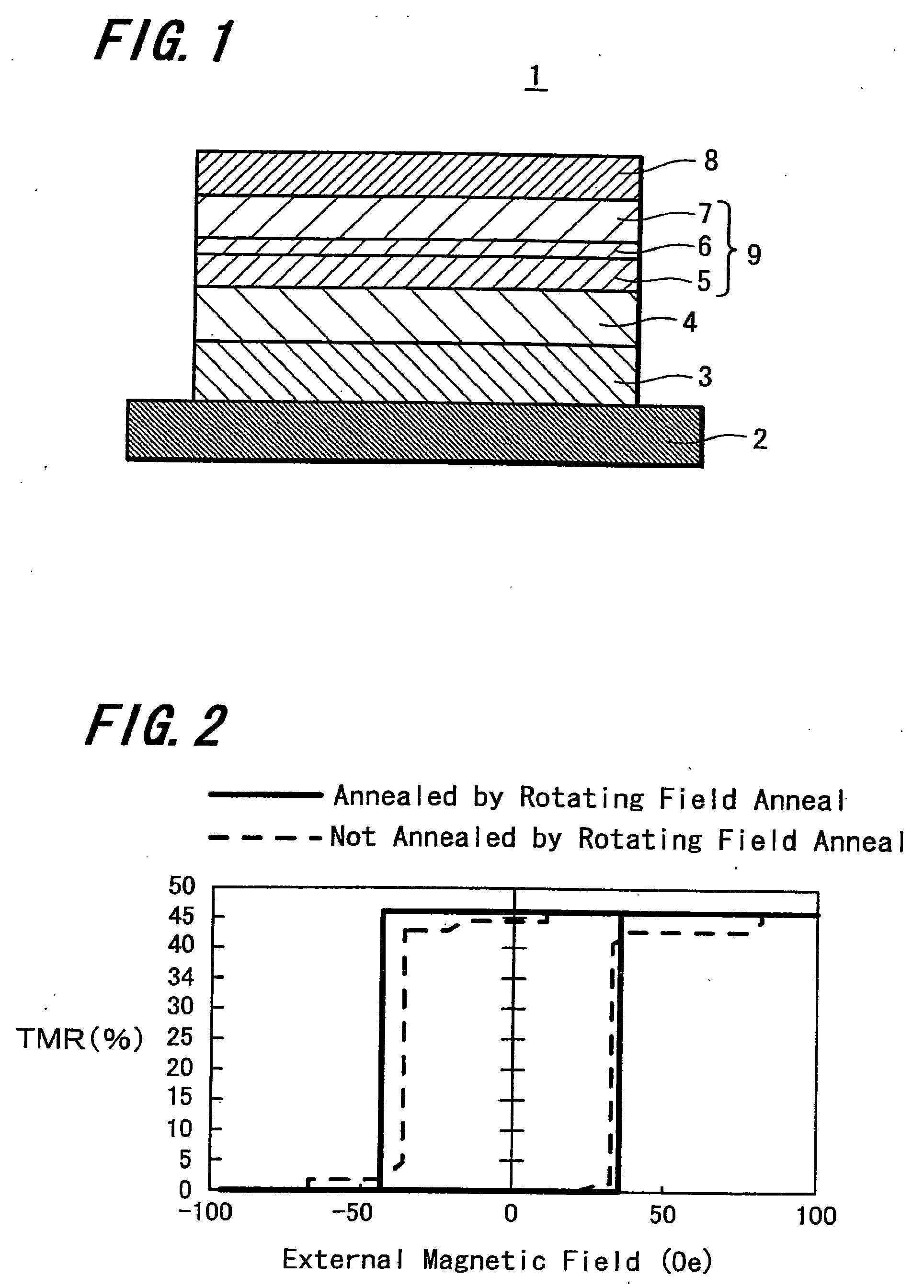
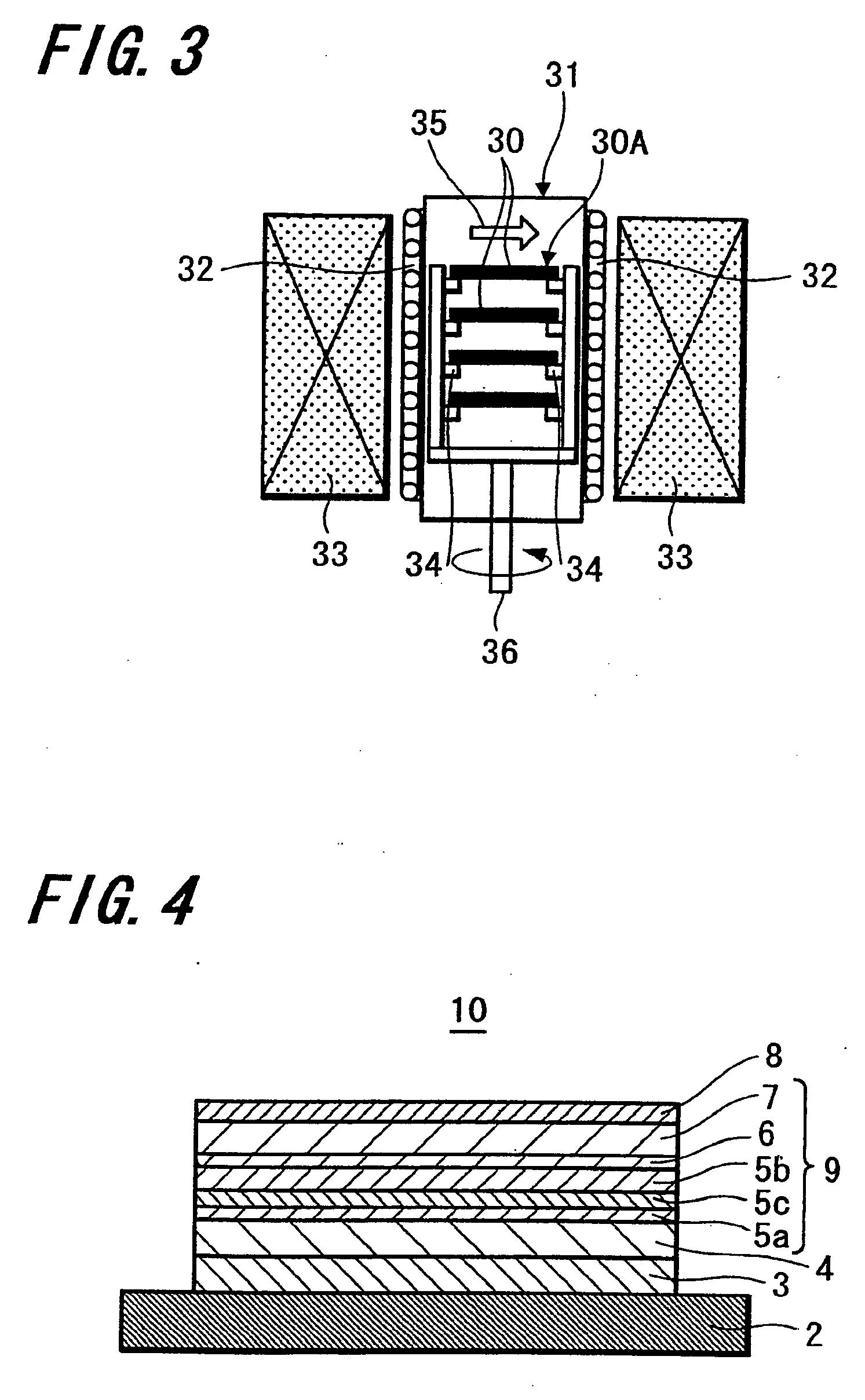
[0040] According to the present invention, there is provided a magnetoresistive effect element having an arrangement in which a pair of ferromagnetic material layers is opposed to each other through an intermediate layer so that a magnetoresistive change is obtained by causing a current to flow in the direction perpendicular to the layer surface. In this magnetoresistive effect element, the ferromagnetic material layers are annealed by anneal including rotating field anneal and the following static field anneal.

[0041] According to the present invention, in the magnetoresistive effect element, at least one of the ferromagnetic material layers is made of an amorphous or microcrystal material.

[0042] According to the present invention, the magnetoresistive effect element is ...


PUM

PropertyMeasurementUnit
thicknessaaaaaaaaaa
temperatureaaaaaaaaaa

Abstract

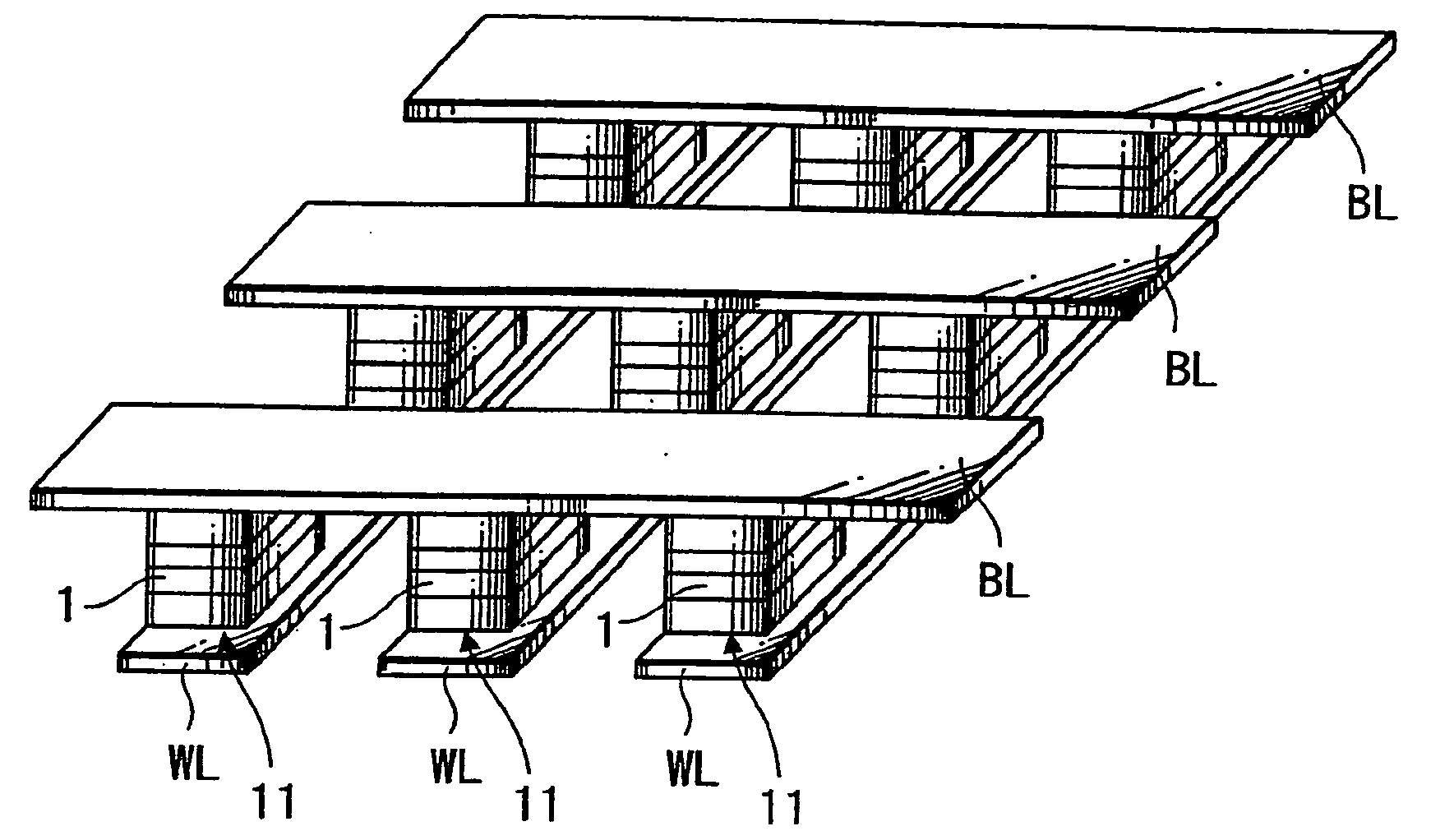
A magnetoresistive effect element (1) has an arrangement in which a pair of ferromagnetic material layers (magnetization fixed layer (5) and magnetization free layer (7)) is opposed to each other through an intermediate layer (6) to obtain a magnetoresistive change by causing a current to flow in the direction perpendicular to the layer surface and in which the ferromagnetic material layers are annealed by anneal including rotating field anneal and the following static field anneal. A magnetic memory device comprises this magnetoresistive effect element (1) and bit lines and word lines sandwiching the magnetoresistive effect element (1) in the thickness direction. When the magnetoresistive effect element (1) and the magnetic memory device are manufactured, the ferromagnetic material layers (5, 7) are annealed by rotating field anneal and the following static field anneal. There are provided the magnetoresistive effect element that can obtain excellent magnetic characteristics by controlling magnetic anisotropies of the ferromagnetic material layers, the magnetic memory device including this magnetoresistive effect element and which may have excellent write characteristics, and methods for manufacturing these magnetoresistive effect element and magnetic memory device.

Description

BACKGROUND OF THE INVENTION [0001] 1. Field of the Invention [0002] The present invention relates to a magnetoresistive effect element having an arrangement for obtaining a magnetoresistive effect change by causing a current to flow in the direction perpendicular to the layer surface and a magnetic memory device including this magnetoresistive effect element. Moreover, the present invention relates to a method of manufacturing this magnetoresistive effect element and a method of manufacturing this magnetic memory device. [0003] 2. Description of the Related Art [0004] As information communication devices, in particular, personal small information communication devices such as portable terminal devices (e.g. personal digital assistants) are widely spreading, it is requested that devices such as memories and logic devices comprising these information communication devices or portable terminal devices should become higher in performance, such as they should become higher in integration...

Claims


Application Information

Patent Timeline
Patent Type & Authority Applications(United States)
IPC IPC(8): G11C11/00G01R33/09H01L27/105G11B5/39G11C11/15H01F10/32H01F41/30H01L21/8246H01L43/08H01L43/12
CPCB82Y10/00B82Y25/00B82Y40/00G11C11/15H01F10/3204Y10T29/49034H01F10/3254H01F41/302H01L27/228H01L43/12H01F10/324H10B61/22H10N50/01
Inventor MIZUGUCHI, TETSUYAHOSOMI, MASANORIOHBA, KAZUHIROBESSHO, KAZUHIROHIGO, YUTAKAYAMAMOTO, TETSUYASONE, TAKEYUKIKANO, HIROSHI
Owner SONY CORP
Learn More