Semiconductor memory device and memory system using same

a memory device and semiconductor technology, applied in the field of semiconductor memory devices, can solve the problems of ineffective adjustment of the delay time between the input data strobe signal and the output data strobe signal, and the inability to arrange the delay for each input data bit and each output data bi

Inactive Publication Date: 2006-08-17
SAMSUNG ELECTRONICS CO LTD
View PDF7 Cites 9 Cited by
  • Summary
  • Abstract
  • Description
  • Claims
  • Application Information

AI Technical Summary

Benefits of technology

[0008] In accordance with an aspect of the present invention, a semiconductor memory device includes: an input data delay time adjustor for varying an input delay time, selecting one bit of n-bit input data, delaying the selected one bit by the input delay time and outputting the delayed bit, in response to a control signal during an input data delay test operation, where n is a predetermined integer; and an output data delay time adjustor for varying an output delay time, selecting one bit of m-bit output data, delaying the selected one bit by the output delay time and outputting the delayed bit, in response to the control signal during an output data delay test operation, where n is a predetermined integer, wherein the input data delay time adjustor is arranged for n-bit input data, and the output data delay time adjustor is arranged for m-bit output data.
[0009] In an exemplary embodiment of the present invention, the semiconductor memory device generates a mode setting command in response to a command for mode setting, and receives a code to generate the control signal in response to the mode setting command.
[0010] In an exemplary embodiment of the present invention, the input data delay time adjustor includes a first switch for transmitting the n-bit input data to a normal input line or a test input line in response to the control signal; a selector and delay for selecting one bit of the n-bit input data outputted from the first switch transmitted to the test input line, delaying the selected bit by the input delay time and outputting the delay bit, in response to the control signal; and a second switch for transmitting data outputted from the first switch or transmitting data outputted from the selector and delay in response to the control signal. The selector and delay includes a first selector for selecting one bit of the n-bit input data outputted from the first switch in response to the control signal; a delay for varying the input delay time and delaying a bit outputted from the first selector by the input delay time in response to the control signal; and a second selector for selecting an output data of the delay and outputting as one bit of the n-bit input data in response to the control signal.
[0011] In an exemplary embodiment of the present invention, the output data delay time adjustor includes a first switch for transmitting the n-bit input data to a normal output line or ...

Problems solved by technology

However, as the operational speed of memory systems has increased, adjusting the delay time of the input data strobe signal and the output data strobe signal has become less effective.
Furthermore, ...

Method used


Image

  • Semiconductor memory device and memory system using same
  • Semiconductor memory device and memory system using same
  • Semiconductor memory device and memory system using same

Examples


Embodiment Construction

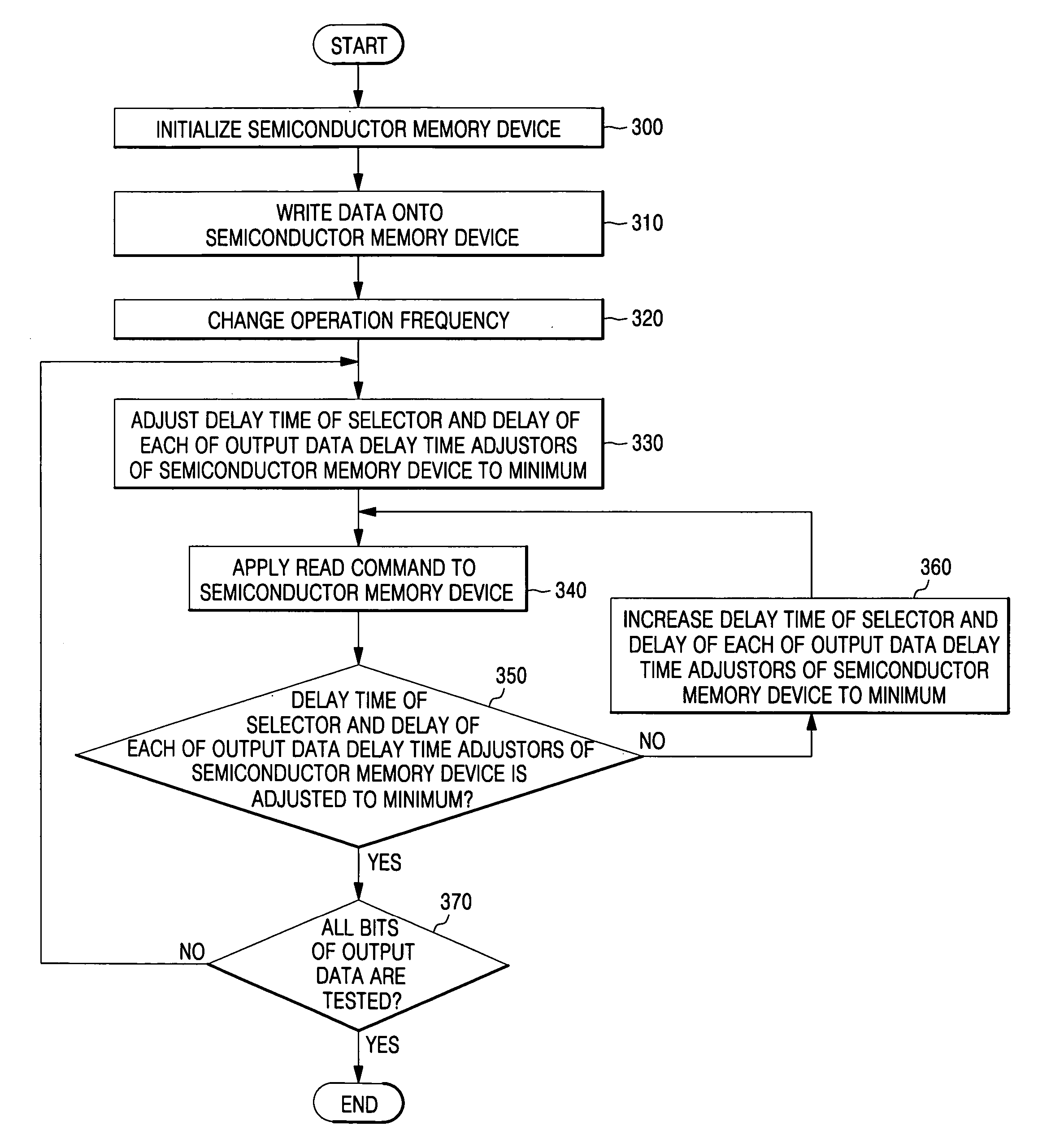
[0021] Hereinafter, the exemplary embodiments of the present invention will be described in detail with reference to the accompanying drawings. In the drawings, the size and relative sizes of layers and regions may be exaggerated for clarity. Like reference numerals refer to similar or identical elements throughout the description of the figures.

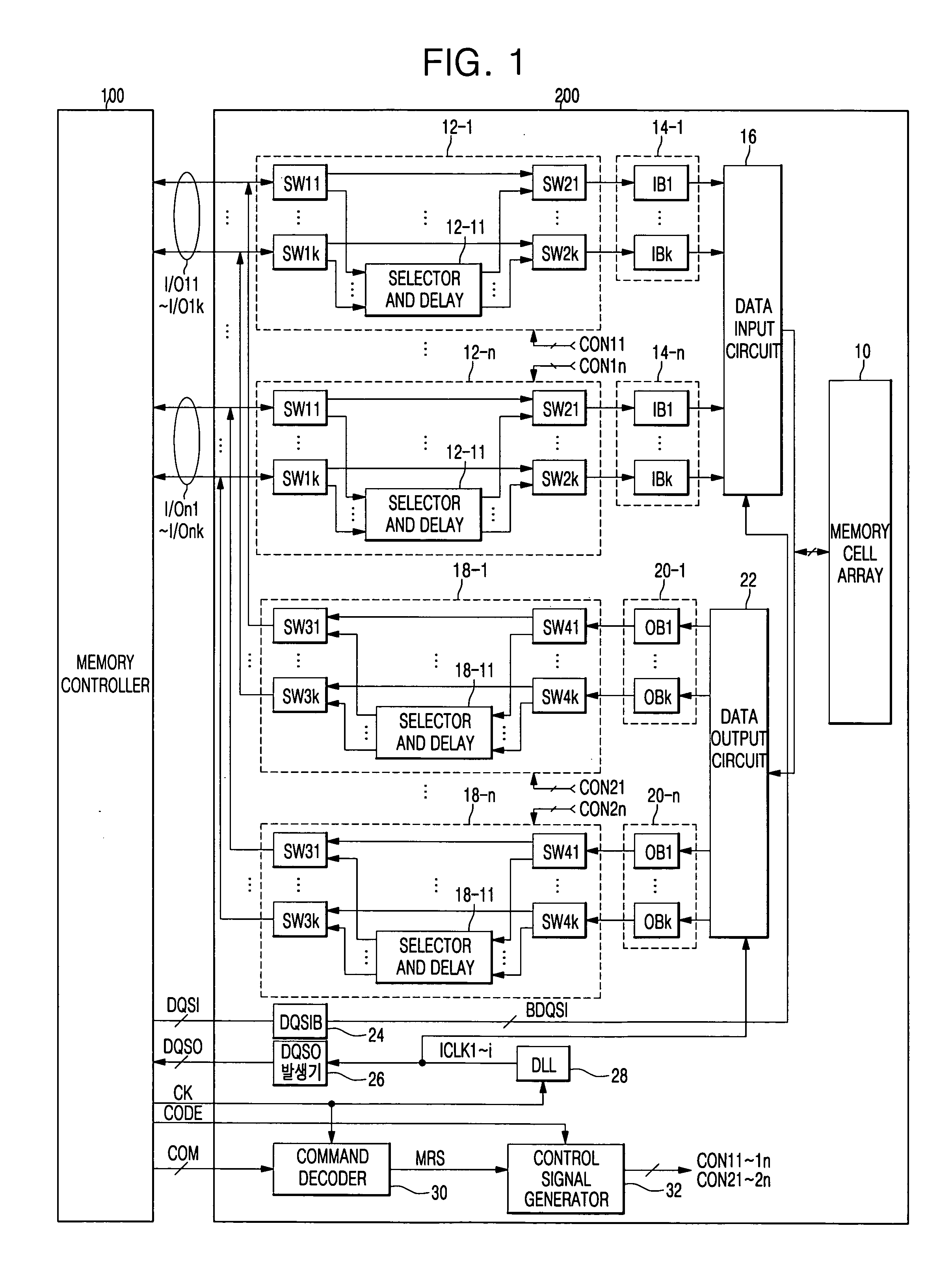
[0022]FIG. 1 is a block diagram illustrating a memory system according to an exemplary embodiment of the present invention. Referring to FIG. 1, the memory system includes a memory controller 100 and a semiconductor memory device 200. The semiconductor memory device 200 includes a memory cell array 10, n input data delay time adjustors 12-1 to 12-n, n data input buffers 14-1 to 14-n, a data input circuit 16, n output data delay time adjustors 18-1 to 18-n, n data output buffers 20-1 to 20-n, a data output circuit 22, an input data strobe signal buffer 24, an output data strobe signal generator 26, a delay locked loop 28, a command decoder 3...


PUM

PropertyMeasurementUnit
Digital informationaaaaaaaaaa
Timeaaaaaaaaaa

Abstract

There is provided a semiconductor memory device and a memory system using the same. The semiconductor memory device includes an input data delay time adjustor for varying an input delay time, selecting one bit of a n-bit input data, delaying the selected one bit by the input delay time and outputting the delayed bit, in response to a control signal during an input data delay test operation; and an output data delay time adjustor for varying an output delay time, selecting one bit of a m-bit output data, delaying the selected one bit by the output delay time and outputting the delayed bit, in response to the control signal during an output data delay test operation, wherein the input data delay time adjustor is arranged for n-bit input data, and wherein the output data delay time adjustor is arranged for m-bit output data.

Description

CROSS-REFERENCE TO RELATED APPLICATION [0001] This application claims priority to Korean Patent Application No. 2005-12054, filed on Feb. 14, 2005, the disclosure of which is herein incorporated by reference in its entirety. BACKGROUND OF THE INVENTION [0002] 1. Technical Field [0003] The present invention relates to a semiconductor memory device and, more particularly, to a semiconductor memory device and a memory system using the same which can reduce a delay time difference between output data bits during a read operation and between input data bits during a write operation. [0004] 2. Description of the Related Art [0005] A typical memory system includes a semiconductor memory device and a memory controller. In general, a delay time difference occurs between data bits outputted from a semiconductor memory device during a read operation and between data bits inputted to the semiconductor memory device during a write operation. [0006] The typical memory system may adjust a delay ti...

Claims


Application Information

Patent Timeline
IPC IPC(8): G06F13/00
CPCG11C7/1051G11C7/1066G11C7/1078G11C7/1093G11C7/20G11C7/22G11C7/222G11C29/02G11C29/022G11C29/023G11C29/028G11C29/50012G11C2207/2254D04H13/00B32B27/12B32B5/24
Inventor LEE, JUNG-JOON
Owner SAMSUNG ELECTRONICS CO LTD
Why Eureka
Try Eureka