Simulation device for integrated circuit

a technology of integrated circuit and simulation device, which is applied in the direction of instruments, computing, electric digital data processing, etc., can solve the problems of reducing the device length of the transistor, adversely affecting the fluctuations in manufacturing conditions, and difficult to set the design margin of the integrated circuit at one pattern, so as to achieve the effect of more accurate design margin and even more accurate design margin

Inactive Publication Date: 2006-08-03
PANASONIC CORP
View PDF1 Cites 8 Cited by
  • Summary
  • Abstract
  • Description
  • Claims
  • Application Information

AI Technical Summary

Benefits of technology

[0016] According to the foregoing structure, the design margin can be appropriately set according to the particular path among the paths between each cell, and the design margin can be more accurate since the circuit information corresponding to the path is inputted. Further, a relation between the design margin and the circuit information can be clarified, which improves a level of efficiency in designing the integrated circuit.
[0019] The particular path is an arbitrary path in an actual circuit block, in which case, more preferably, when a path having a large delay variation is selected as the arbitrary path so that the design margin to be set can be prevented from resulting in an excess or underestimate and thereby is given at a high accuracy
[0024] Further, in the foregoing structure comprising a third input unit for providing a delay variation distribution by actual measurements to the net list, it is preferable that the design margin can be set in comparison of the delay variation distribution calculated by the execution of the simulation with the delay variation distribution by the actual measurements, in which case the design margin can be more accurately set.
[0025] Further, it is preferable that the variation information relating to the gate lengths, gate widths and the like of the transistors be corrected so that the delay variation distribution obtained in the simulation is consistent with the delay variation distribution by the actual measurements, in which case the design margin can be even more accurately set.
[0029] As so far described, according to the present invention, the design margin can be appropriately set corresponding to the different paths, and further, the design margin can be more accurate by inputting the circuit information. Further, the relation between the design margin and the circuit information can be clarified, which gives a large affect on the designing process of the integrated circuit.

Problems solved by technology

In a manufacturing process of an integrated circuit, manufacturing conditions unavoidably fluctuate, and the fluctuations generated in the manufacturing conditions have an effect on shapes and physical conditions of circuit elements, thereby generating variations in characteristics of the integrated circuit.
Though a device length of a transistor tends to be reduced along with minimization in a rapid progress of the integrated circuit in order to improve a performance thereof, the minimization that is increasingly advanced (reduction of the device length of the transistor) adversely enlarges the fluctuations in the manufacturing conditions.
Thus, the advancement of the minimization can be a barrier for homogenizing the characteristics of the integrated circuit.
However, there are many types of the integrated circuit, and a cell structure differs in each of the types, which makes it difficult to set the design margin of the integrated circuit at one pattern.

Method used


Image

  • Simulation device for integrated circuit
  • Simulation device for integrated circuit
  • Simulation device for integrated circuit

Examples


embodiment 1

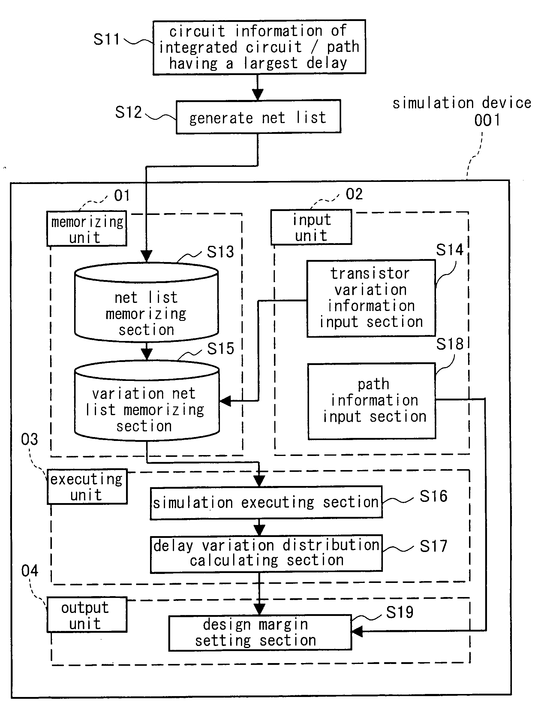
[0046]FIG. 1 is a block diagram illustrating a structure of a simulation device 001 for an integrated circuit according to an embodiment 1 of the present invention. The simulation device 001 comprises four components, which are a memory unit 01, an input unit 02, an execute unit 03 and an output unit 04. Below is described a method of simulating the integrated circuit using the simulation device 001.

[0047] First, a path having the largest delay, that is a critical path, is selected among the flip-flops of the circuit and the paths of the flip-flop circuits as an information of the integrated circuit to be inputted to the simulation device 001 (Step S11). Then, a net list of the path selected in the Step S11 is prepared (Step S12), and the prepared net list is stored in the memory unit 01 (Step S13), wherein an operation of the Step S13 is executed by a net list memory section of the memory unit 01. The net list memory section corresponds to the first memory unit according to the pr...

embodiment 2

[0058] Next, a simulation device 002 for an integrated circuit according to an embodiment 2 of the present invention is described. In the embodiment 1, the critical path having the largest delay in the paths between the flip-flop circuits is used as the information of the integrated circuit used for the simulation. In contrast to the embodiment 1, a net list of an arbitrary path in an actual circuit block is used in the embodiment 2, wherein the design margin can be set in view of any influence from the path on the delay variation.

[0059]FIG. 5 is a block diagram illustrating a structure of the simulation device 002 for the integrated circuit according to the embodiment 2. The reference numerals shown in FIG. 5 are identical to those shown in FIG. 1 (embodiment 1), and the same reference numerals denote the same components. Any component described in the embodiment 1 is not described in the present embodiment again. Below is described a feature on structure of the embodiment 2.

[006...

embodiment 3

[0061] Next, a simulation device 003 for an integrated circuit according to an embodiment 3 of the present invention is described. In the embodiment 2, an arbitrary path in the actual circuit block is used as the information of the integrated circuit used in the simulation. In contrast to the embodiment 2, net lists of a plurality of arbitrary paths in the actual circuit block are used in the embodiment 3 so that the design margin can be set up in view of any influence from the plurality of paths on the delay variation.

[0062]FIG. 6 is a block diagram illustrating a structure of the simulation device 003 for the integrated circuit according to the embodiment 3. The reference numerals shown in FIG. 6 are identical to those shown in FIG. 1 (embodiment 1), and the same reference numerals denote the same components. Any component described in the embodiment 1 is not described in the present embodiment again. Below is described a feature on structure of the embodiment 3.

[0063] The plura...


PUM


Abstract

A simulation device for an integrated circuit according to the present invention comprises a first memory unit, a first input unit, a second memory unit, an execute unit, a second input unit and an output unit. A net list of a particular path in inter-cell paths in the integrated circuit comprising a plurality of synchronizing circuit cells is stored in the first memory unit. The first input unit appends a variation information relating to gate lengths, gate widths and the like of transistors to the net list stored in the first memory unit. The variation net list to which the variation information is appended by the first input unit is stored in the second memory unit. The execute unit executes a simulation using the variation net list stored in the second memory unit to thereby calculate a delay variation distribution. The second input unit appends a circuit information to the path. The output unit sets and outputs a design margin of the circuit based on the delay variation distribution calculated by the execute unit and the circuit information appended by the second input unit.

Description

BACKGROUND OF THE INVENTION [0001] 1. Field of the Invention [0002] The present invention relates to a simulation device for setting a design margin of a semiconductor integrated circuit and a method of designing an integrated circuit using the simulation. [0003] 2. Description of the Related Art [0004] In a manufacturing process of an integrated circuit, manufacturing conditions unavoidably fluctuate, and the fluctuations generated in the manufacturing conditions have an effect on shapes and physical conditions of circuit elements, thereby generating variations in characteristics of the integrated circuit. Though a device length of a transistor tends to be reduced along with minimization in a rapid progress of the integrated circuit in order to improve a performance thereof, the minimization that is increasingly advanced (reduction of the device length of the transistor) adversely enlarges the fluctuations in the manufacturing conditions. Thus, the advancement of the minimization c...

Claims


Application Information

Patent Timeline
Patent Type & Authority Applications(United States)
IPC IPC(8): G06F17/50
CPCG06F17/5022G06F30/33
Inventor SUMIKAWA, TAKASHI
Owner PANASONIC CORP
Why Eureka
Try Eureka