EUV lithography filter

a lithography filter and lithography technology, applied in the field of semiconductor devices, can solve the problems of inability to replace frequently, inability to meet the needs of users, and high cost of optic mirrors, so as to achieve the effect of enabling the viability of euv lithography, reducing the accumulation of debris, and reducing damage to optical components

Inactive Publication Date: 2006-07-20
INFINEON TECH AG +1
View PDF18 Cites 56 Cited by
  • Summary
  • Abstract
  • Description
  • Claims
  • Application Information

AI Technical Summary

Benefits of technology

[0016] In accordance with another preferred embodiment of the present invention, a method of filtering debris in an EUV lithography system having at least one optical component includes disposing a filter proximate the at least one optical component, the filter comprising a layer of nanotube material with support material disposed on at least one side of the nanotube material, and generating EUV radiation, wherein generating the EUV radiation produces debris. The filter is adapted to reduce accumulation of the debris on the optical component and reduce damage to the optical component.
[0017] Advantages of embodiments of the present invention include enabling the viability of EUV lithography in high volume production environments by increasing the lifetime of EUV lithography equipment. The reduction

Problems solved by technology

However, in the process of generating EUV radiation, in these methods, additional unwanted radiation and debris are produced.
The optic mirror is costly, has a certain useful lifetime, and cannot be replaced frequently, and thus needs to be protected from the debris.
The kinetic energy of the debris can be very high and may cause erosion of the EUV system collecting optics, such as a grazing incidence collector, multilayer mirrors, or near normal incident Bragg reflector mirrors used in the sources as EUV light collectors.
The highly charged ion debris can be very damaging to EUV system collecting optics surfaces, even at very low kinetic energies.
This erosion is caused by potential energy sputtering of the highly charged ion debris.
The damage caused by this kind of debris to the EUV collecting optics in EUV sources significantly reduces the lifetime of the EUV lenses and mirrors, and increases cost of ownership (COO) for EUV sources and EUV lithography systems.
Mitigating debris to prevent the debris from reaching the collecting optics is considered one of the largest challenges in the development of EUV lithography.
Extending

Method used


Image

  • EUV lithography filter
  • EUV lithography filter
  • EUV lithography filter

Examples


Embodiment Construction

[0039] The making and using of the presently preferred embodiments are discussed in detail below. It should be appreciated, however, that the present invention provides many applicable inventive concepts that can be embodied in a wide variety of specific contexts. The specific embodiments discussed are merely illustrative of specific ways to make and use the invention, and do not limit the scope of the invention.

[0040] The present invention will be described with respect to preferred embodiments in a specific context, namely filters for use in EUV lithography systems. The invention may also be applied, however, to other applications that require filters, such as in other semiconductor lithography systems or in other systems with optical devices that need protection from debris.

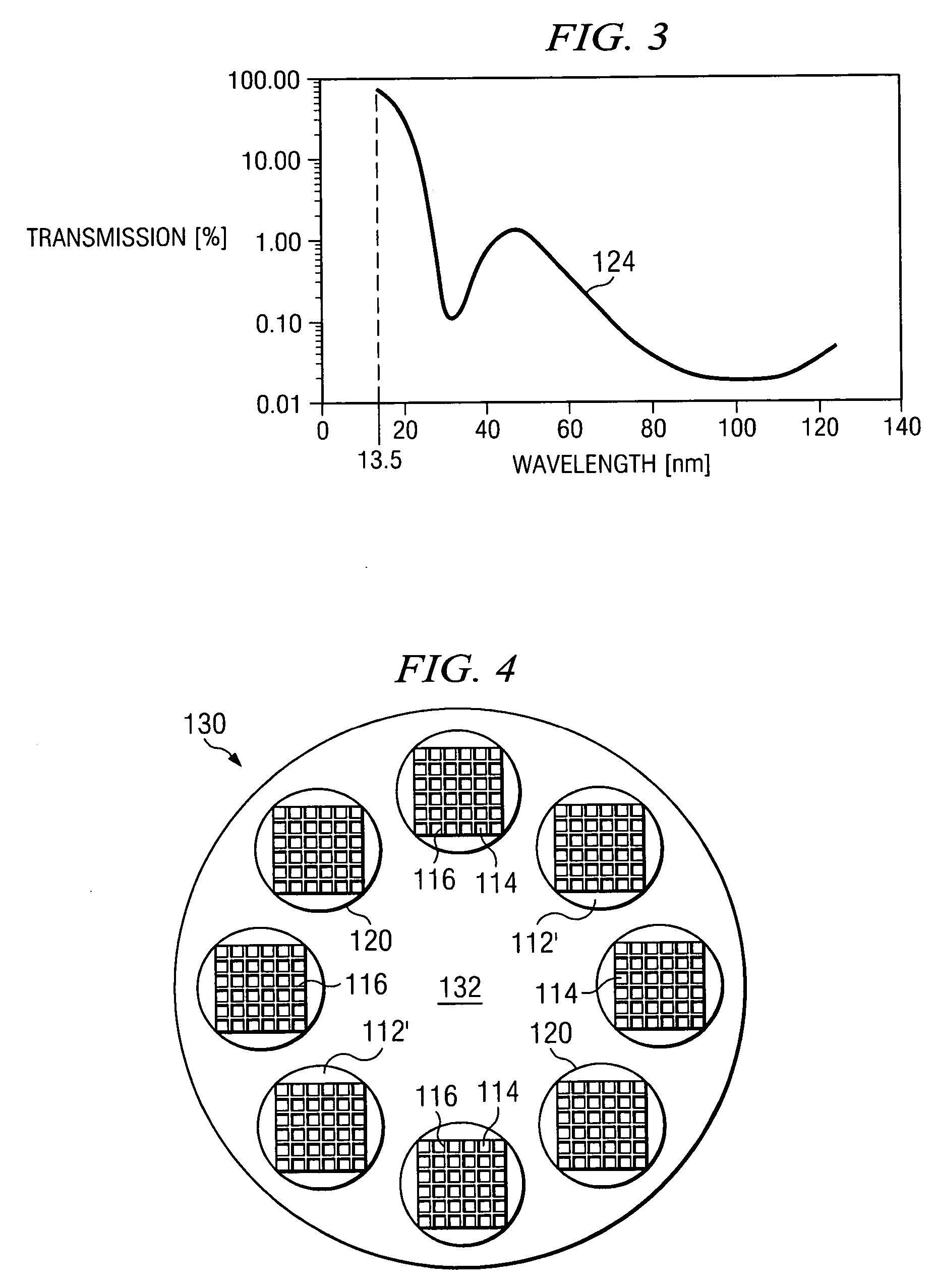
[0041] The novel debris mitigation device or filter in accordance with embodiments of the present invention comprises a highly EUV transparent yet stable nanotube material sandwiched between two layers of st...


PUM


Abstract

Filters for EUV lithography, methods of manufacture thereof, and methods of filtering in an EUV lithography system are disclosed. The filter comprises a nanotube material layer sandwiched by two thin material layers that are highly transmissive and provide structural support for the nanotube material layer. The filter is supported on at least one side by a patterned structural support. The filter mitigates debris, provides spectral purity filtering, or both.

Description

TECHNICAL FIELD [0001] The present invention relates generally to the manufacturing of semiconductor devices, and more particularly to filters for use with extreme ultraviolet lithography (EUVL) systems. BACKGROUND [0002] Semiconductor devices are manufactured by depositing many different types of material layers over a semiconductor workpiece or wafer, and patterning the various material layers using lithography. The material layers typically comprise thin films of conductive, semiconductive, and insulating materials that are patterned and etched to form integrated circuits (IC's). [0003] For many years in the semiconductor industry, optical lithography techniques such as contact printing, proximity printing, and projection printing have been used to pattern material layers of integrated circuits. Projection printing is commonly used in the semiconductor industry using wavelengths of 248 nm or 193 nm, as examples. At such wavelengths, lens projection systems and transmission lithog...

Claims


Application Information

Patent Timeline
IPC IPC(8): G03C5/00G03B27/42
CPCG02B5/208G03F7/70191G03F7/70575G03F7/70825G03F7/70908G03F7/70916G03F7/70958G21K1/10
Inventor WURM, STEFANBAKSHI, VIVEK
Owner INFINEON TECH AG
Why Eureka
Try Eureka