Readout circuit for semiconductor storage device

a semiconductor storage device and readout circuit technology, applied in semiconductor devices, digital storage, instruments, etc., can solve the problems of increasing circuit area, deteriorating cell yield, and difficult to generate uniform insulating film, so as to reduce device area and power consumption, prevent the production yield from being lowered, and high-speed readout

Inactive Publication Date: 2006-07-20
NEC CORP
View PDF5 Cites 9 Cited by
  • Summary
  • Abstract
  • Description
  • Claims
  • Application Information

AI Technical Summary

Benefits of technology

[0014] In view of the above-depicted status of the art, it is an object of the present invention to provide a readout circuit for a non-volatile semiconductor storage device, exploiting a tunnel magneto-resistive device, in which it is possible to reduce the area of the device and power consumption, to achieve high-speed readout and to prevent the production yield from being lowered as a result of variations in the resistance value of the TMR.

Problems solved by technology

It is however difficult to generate a uniform insulating film with film thickness variations of the order of an atomic layer.
Thus, the MRAM of the above-described conventional art suffers from the problem that, even though the storage state of the memory cell is ‘1’ or ‘0’, the voltage obtained from the memory cell becomes larger or smaller than the voltage obtained from the reference cell, respectively, thus deteriorating the cell yield.
However, this needs a register circuit for several bits, thus increasing the circuit area.

Method used


Image

  • Readout circuit for semiconductor storage device
  • Readout circuit for semiconductor storage device
  • Readout circuit for semiconductor storage device

Examples


embodiments

[0051] By referring to the drawings, preferred embodiments of the present invention will be explained in detail.

first embodiment

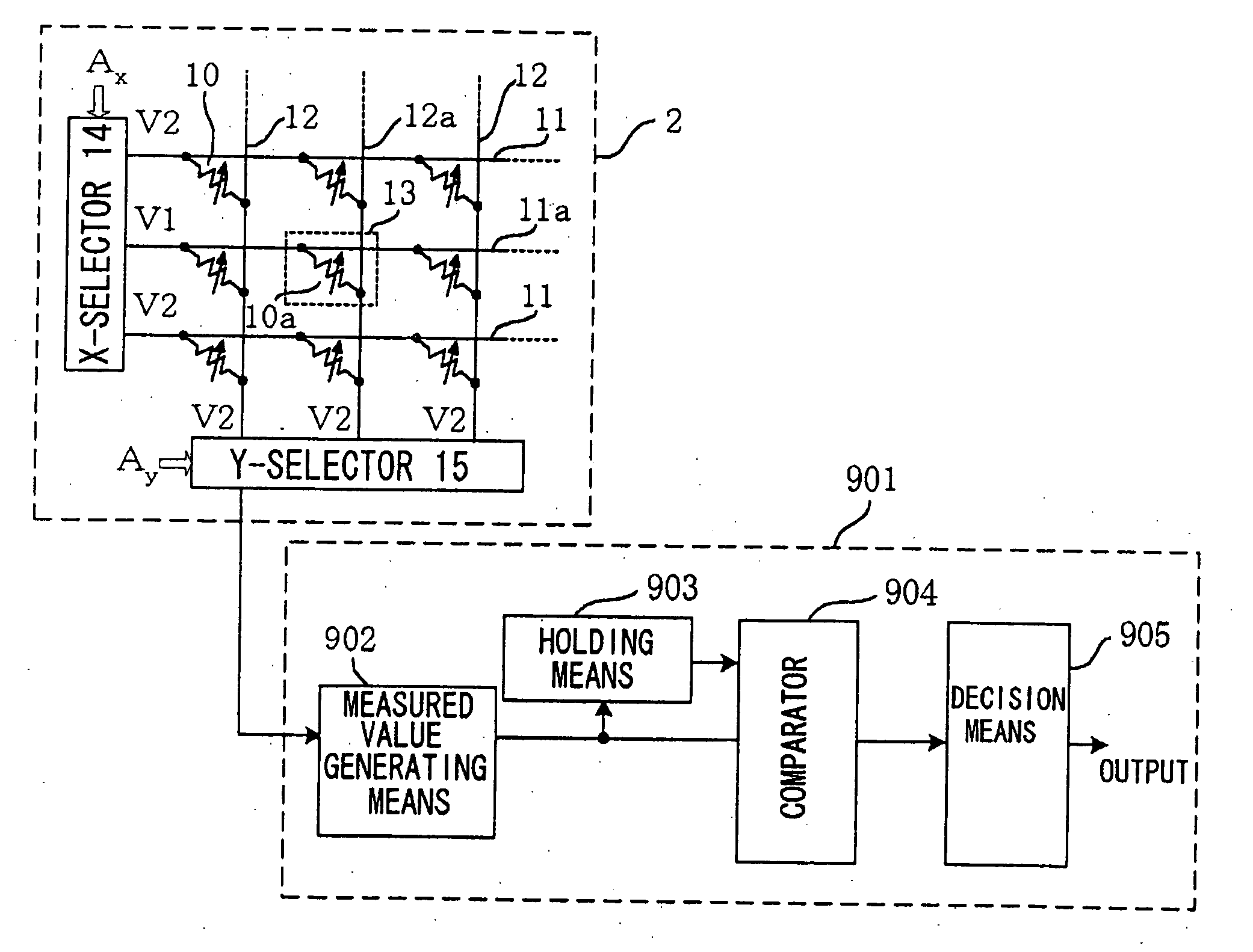
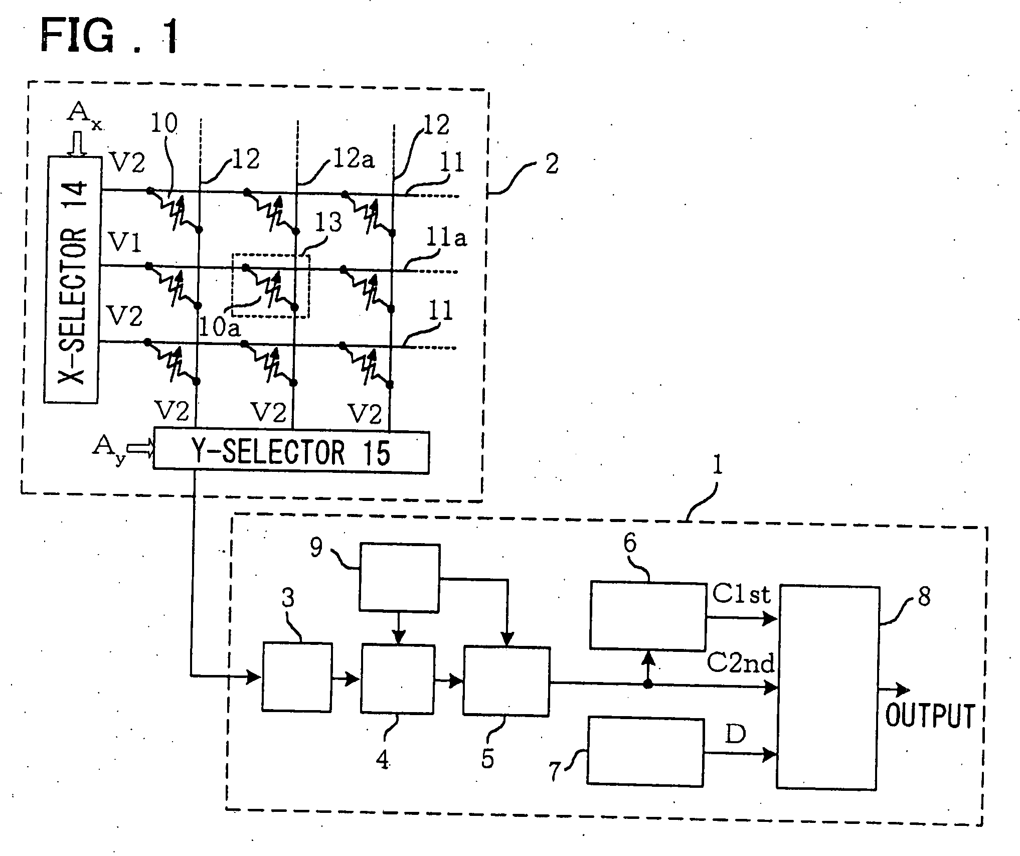
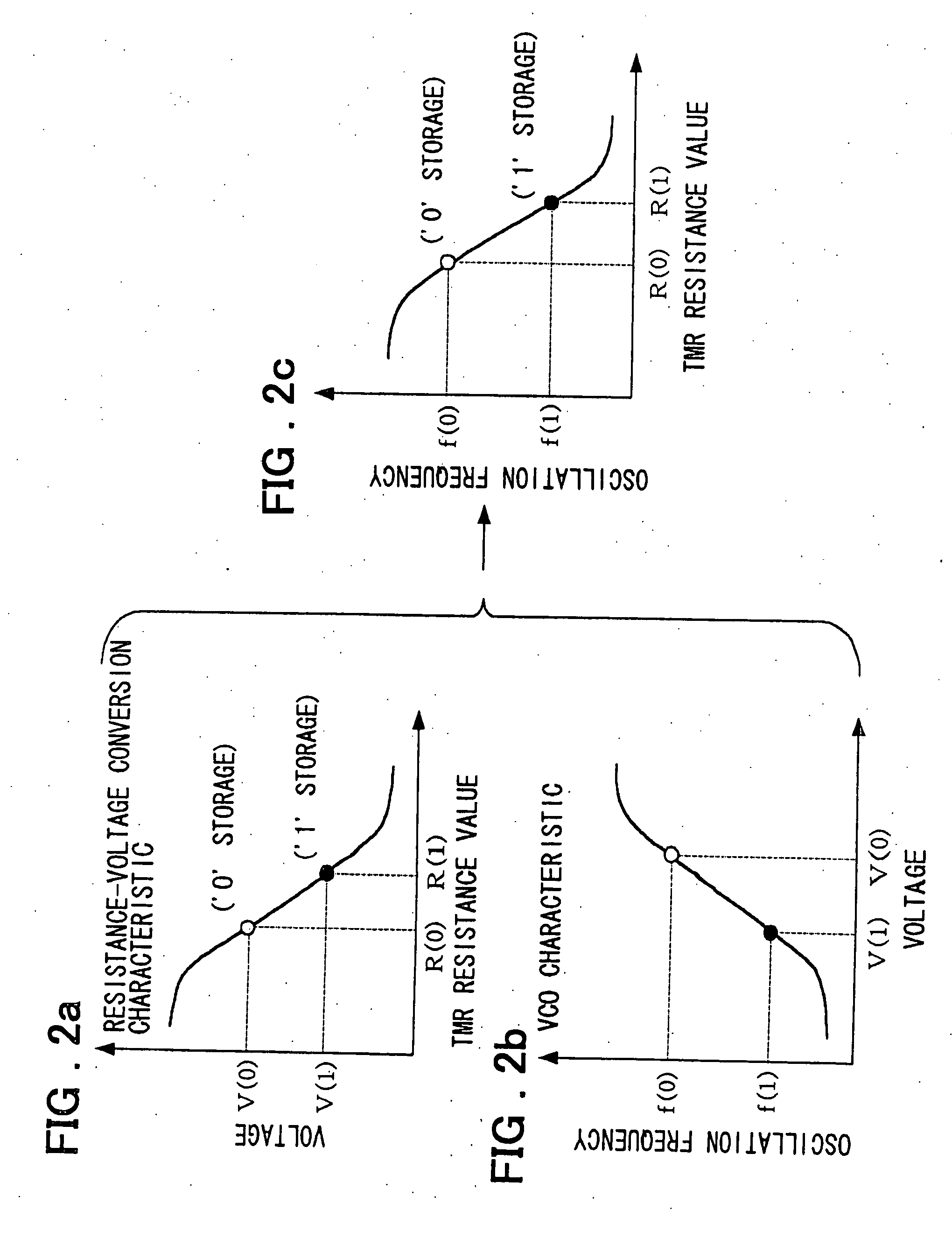
[0052]FIG. 1 depicts a block circuit diagram of an MRAM used in a first embodiment of the present invention. Referring to FIG. 1, the MRAM of the present embodiment includes a memory cell array 2 and a readout circuit 1. The memory cell array 2 is the same as that explained with reference to FIG. 26 and hence is not explained here. Only the current flowing through the TMR 10a is supplied to the readout circuit 1. This readout circuit 1 includes a preamplifier 3 for converting the current flowing through the TMR of the selected cell into the voltage in an amplifying fashion, a VCO (voltage-controlled oscillator) 4 for oscillating at a frequency proportionate to the output voltage of the preamplifier 3, a counter 5 for counting the number of pulses of the VCO 4 during an optional period, a readout value register 6 for storage of an output value of the counter 5, a reference value register 7 for pre-storage of a reference decision value, a decision means 8 for verifying the storage sta...

second embodiment

[0063]FIG. 7 depicts a block circuit diagram of a readout circuit of the second embodiment of the present invention. Referring to FIG. 7, a readout circuit 101 of the present embodiment includes a gain-controllable preamplifier 103A for amplifying the current flowing through the selected cell into voltage and for controlling the conversion gain, a VCO 104 oscillating at a frequency proportionate to the output voltage of the gain-controllable preamplifier 103A, a counter 105 for counting the number of oscillation pulses of the VCO 104 during an optional preset period, and a readout value register 106 for storage of an output value of the counter 105. The readout circuit also includes a decision means 108 for verifying the previous storage state in the selected cell from the output values of the readout value register 106 and the counter 105, and a control circuit 109 for controlling the operation of the readout circuit 101. In FIG. 7, the component parts having the functions which ar...


PUM


Abstract

By first readout, the current input from a selected cell 13 is converted by a preamplifier 3 and a VCO 4 into pulses of a frequency inversely proportionate to the current value, and the number of the pulses within a preset time interval is counted by a counter 5 so as to be stored in a readout value register 6. A selected cell is then written to one of two storage states, and second readout is then carried out. The storage state of the selected cell is verified by comparing a count value of the counter for the second readout, a count value for the first readout as stored in a readout value register and a reference value stored in a reference value register 7 to one another. By the use of the VCO, the integrating capacitor for the current or reference pulse generating means, so far needed, may be eliminated to assure a small area, low power consumption and fast readout.

Description

CROSS-REFERENCE TO RELATED APPLICATIONS [0001] The present application is a divisional application of application Ser. No. 10 / 934,599 filed on Sep. 3, 2004, which is a continuation of PCT / JP03 / 02094 filed Feb. 26, 2003.TECHNICAL FIELD [0002] This invention relates to a readout circuit for a semiconductor storage device, in particular a readout circuit for a semiconductor storage device having a memory cell including a tunnel magneto-resistive element. BACKGROUND ART [0003]FIGS. 21a and 21b show the structure and the principle of a tunnel magneto-resistive element, referred to below as TMR. Referring to FIG. 21a, a TMR 610 includes an insulating film 652 and magnetic layers 653, 654 formed on both sides thereof. The insulating film 652 has a thickness of 10 to 20 Å, while that of each of the magnetic layers 653, 654 is on the order of 50 Å. One 653 of the two magnetic layers 653, 654 is termed a pin layer having its direction of magnetization not changed by the application of the mag...

Claims


Application Information

Patent Timeline
Patent Type & Authority Applications(United States)
IPC IPC(8): G11C7/00G11C7/06G11C11/14G11C11/15G11C11/16G11C16/04H01L21/8246H01L27/105H01L43/08
CPCG11C7/06G11C11/16G11C13/004G11C13/0061G11C2013/0054G11C2013/0057G11C2207/066G11C11/1673G11C2013/0047
Inventor SAKIMURA, NOBORUHONDA, TAKESHISUGIBAYASHI, TADAHIKO
Owner NEC CORP
Why Eureka
Try Eureka