
Method of manufacturing a semiconductor device having a photon absorption layer to prevent plasma damage

Inactive Publication Date: 2006-07-06
SAMSUNG ELECTRONICS CO LTD
View PDF7 Cites 1 Cited by
  • Summary
  • Abstract
  • Description
  • Claims
  • Application Information

AI Technical Summary

Benefits of technology

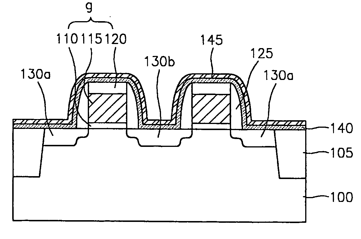
[0011] The present invention is directed to preventing or minimizing the PID problem in gate oxide during the HDP deposition process of the interlayer dielectric layer. One of the main features of the present invention involves providing a means for absorbing the photons, in the wavelength range of 300-1200 nm, generated during the HDP process, by inserting a photon absorption layer, which is made of a material having a lower bandgap energy than SiN or SiON.
[0013] According to a feature of an embodiment of the present invention, there is provided MOSFET semiconductor device structures for preventing plasma-induced-damage in the gate oxide during high-density plasma deposition of an interlayer dielectric layer.
[0014] The present invention also provides methods of fabricating MOSFET semiconductor device structures intended for preventing plasma-induced-damage in the gate oxide during high-density plasma deposition of an interlayer dielectric layer.

Problems solved by technology

When these photons are absorbed by the gate oxide, they induce damage.
The PID degrades gate oxide reliability and may increase the probability of device failure.
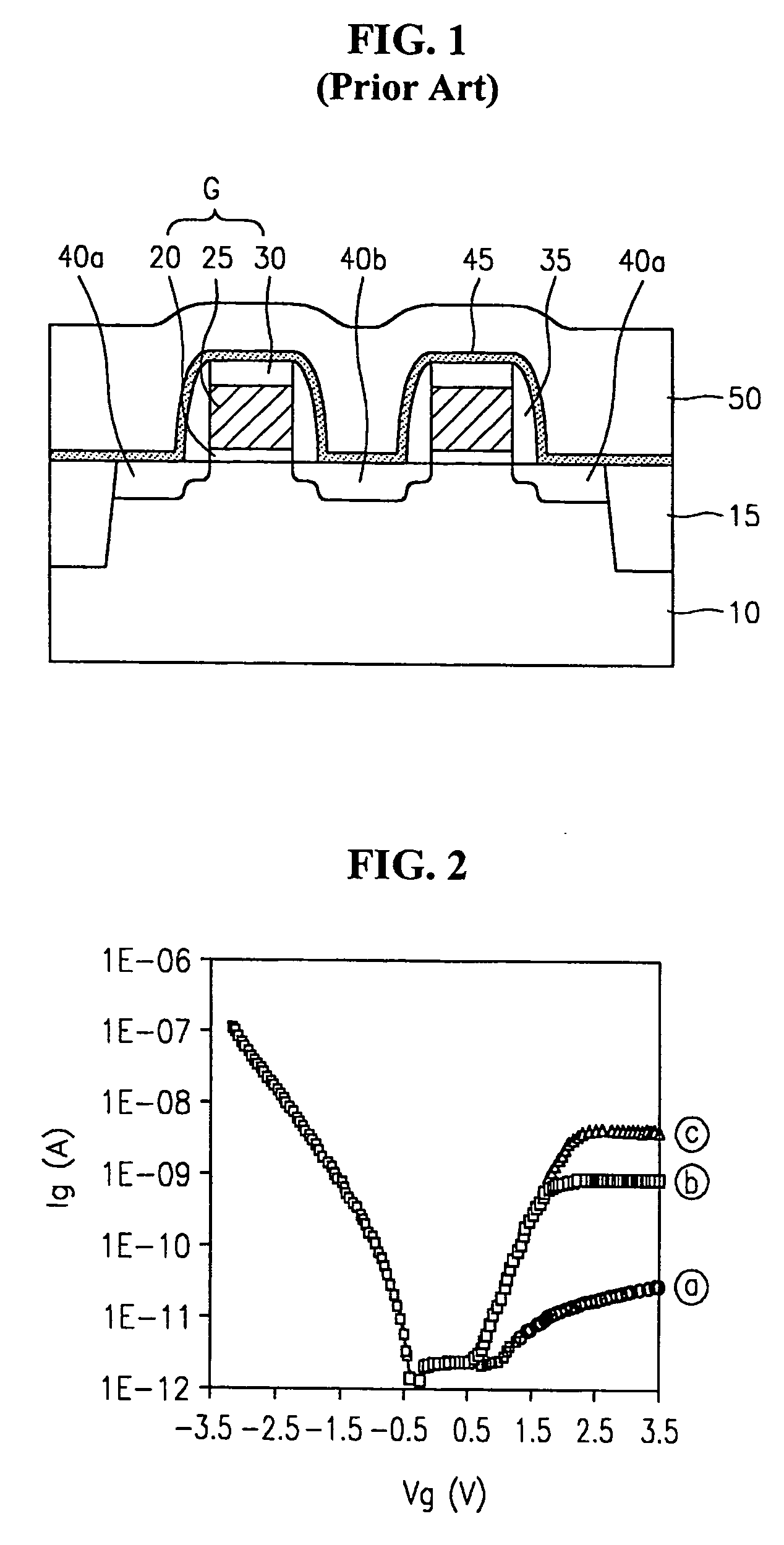
The PID in gate oxide leads to gate leakage current.
The HDP deposition and etching processes are associated with greater amounts of photons, which in turn has the potential of more easily penetrating through the various layers of gate stack, and thereby inflicting more damage to the gate oxide.
The HDP process, however, has a problem in that it generates photons at a high density level.

Method used


Image

  • Method of manufacturing a semiconductor device having a photon absorption layer to prevent plasma damage
  • Method of manufacturing a semiconductor device having a photon absorption layer to prevent plasma damage
  • Method of manufacturing a semiconductor device having a photon absorption layer to prevent plasma damage

Examples


Embodiment Construction

[0034] The present invention will now be described more fully hereinafter with reference to the accompanying drawings, in which preferred embodiments of the invention are shown. The invention may, however, be embodied in different forms and should not be construed as limited to the embodiments set forth herein. Rather, these embodiments are provided so that this disclosure will be thorough and complete, and will fully convey the scope of the invention to those skilled in the art. In the drawings, the thickness of layers and regions are exaggerated for clarity.

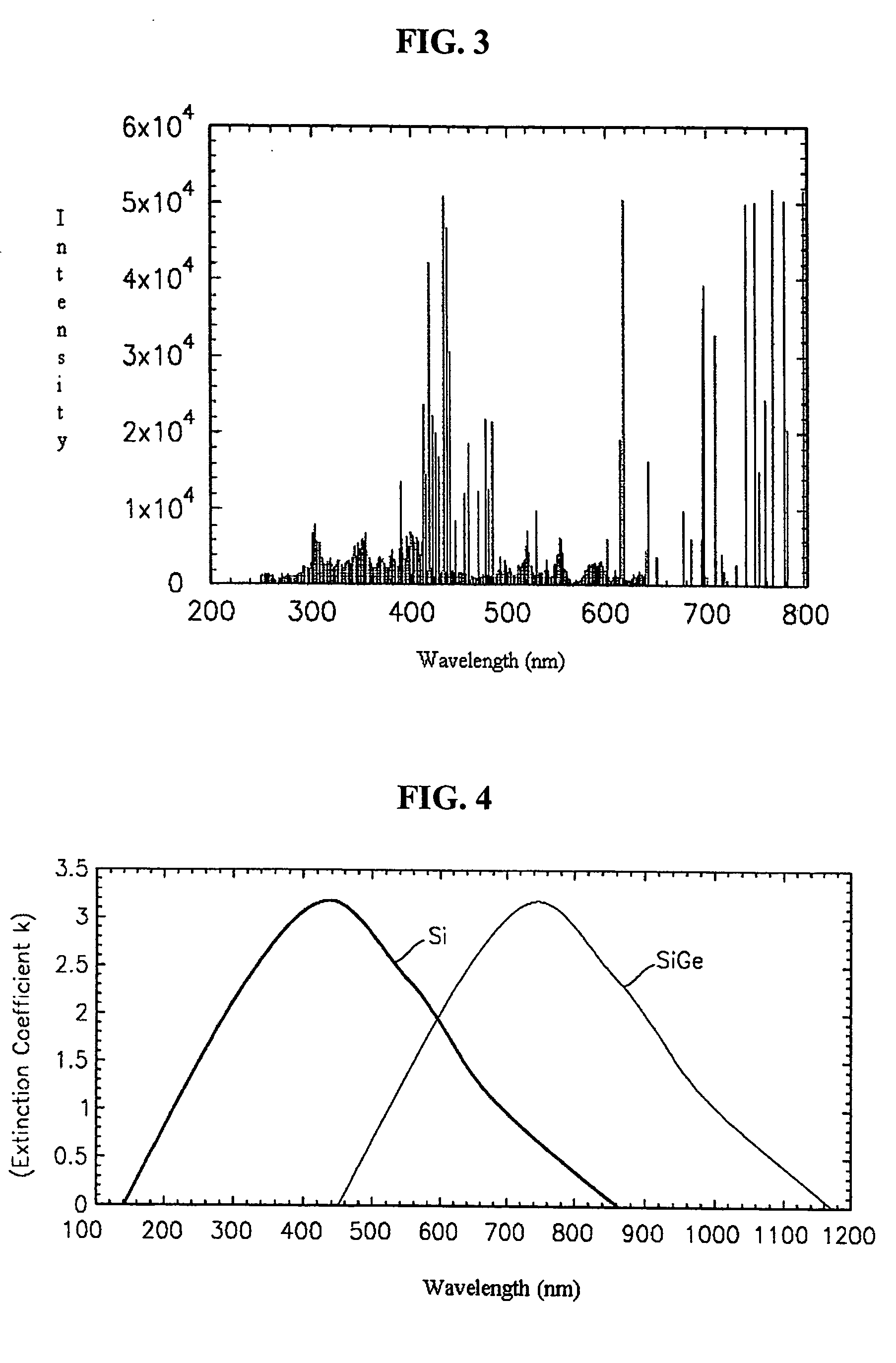
[0035] The bandgap energy of a silicon layer is approximately 1.1 eV at room temperature. Silicon has a nonzero extinction coefficient k in a wavelength range of 300-800 nm. For Si, a peak k value is about 3.2 at approximately 430 nm, with the k value falling on both decreasing and increasing wavelengths, as shown in FIG. 4. The k value decreases to less than 2 in a wavelength range of 600-800 nm.

[0036] Conventionally, absorp...


PUM


Abstract

A MOSFET device structure and a method of manufacturing the same, in which a photon absorption layer is formed over a gate structure and a substrate in order to avoid plasma induced damage to the gate oxide during high density plasma deposition of a interlayer dielectric layer. The device structure may include an etch stop layer below the photon absorption layer. The photon absorption layer is formed entirely of silicon germanium or it may be a multi-layer formed of a silicon layer and a silicon germanium layer. In the multi-layer structure the silicon germanium layer may be formed on top of the silicon layer or vice-versa. The silicon germanium layer may be formed by implanting germanium ions into a silicon layer or by an epitaxial growth of the silicon germanium alloy layer. In the photon absorption layer the germanium may be substituted by another element whose band gap energy is less than that of silicon.

Description

CROSS REFERENCE TO RELATED APPLICATION(S) [0001] This is a divisional application based on pending application Ser. No. 10 / 740,570, filed Dec. 22, 2003, the entire contents of which is hereby incorporated by reference.BACKGROUND OF THE INVENTION [0002] 1. Field of the Invention [0003] The present invention relates to a semiconductor device structure and a processing method thereof for preventing plasma-induced-damage to the device during plasma processing. More particularly, the present invention is directed to a MOSFET semiconductor device structure and a processing method thereof for preventing plasma-induced-damage to the gate oxide during high-density plasma deposition of an interlayer dielectric layer. [0004] 2. Description of the Related Art [0005] As ultra large scale integration (ULSI) technology has progressed, the use of plasma processes for etching and deposition has increased. Plasma deposition is a preferred process because it offers a good thermal budget control due to...

Claims


Application Information

Patent Timeline
IPC IPC(8): H01L33/00H01L21/768H01L21/00H01L21/28H01L21/336H01L21/8234H01L23/522H01L23/532H01L29/78
CPCH01L21/265H01L21/76825H01L21/76832H01L21/76834H01L21/76837H01L2924/0002H01L29/6659H01L2924/00
Inventor SONG, SEUNG-CHUL
Owner SAMSUNG ELECTRONICS CO LTD
Learn More