Vertical alignment liquid crystal display device

Active Publication Date: 2006-06-29
ORTUS TECH
View PDF98 Cites 49 Cited by
  • Summary
  • Abstract
  • Description
  • Claims
  • Application Information

AI Technical Summary

Benefits of technology

[0009] An object of the present invention is to provide a vertical alignment active matrix liquid crystal display device which can achieve bright display and a wide view angle with no display unevenness, and can display an image of a high-quality by aligning the liquid crystal molecules in each pixel stably into the lying alignment by applying a voltage.
[0018] The liquid crystal display device according to the first aspect provides each pixel electrode with at least one slit for separating the pixel electrode into a plurality of electrode portions to divide one pixel into a plurality of sub-pixels, by eliminating a part of the pixel electrode with a connecting portion kept that has a predetermined width for connecting sub-pixels of adjoining electrode portions of the pixel electrode, and has the width of the connecting portion formed to be smaller than ⅕ of the width of the pixel electrode which width of the pixel electrode runs in the direction in which the slit is formed. Thus, when a voltage is applied, the liquid crystal molecules in each pixel can be stably aligned into a lying alignment, sub-pixel by sub-pixel corresponding to the plurality of electrode portions, from the periphery of the sub-pixels toward the center of the sub-pixels, without being influenced by the alignment of the liquid crystal molecules in the other sub-pixels corresponding to the adjoining electrode portion. Accordingly, a high-quality image with no display roughness can be displayed, and a bright image can be displayed because the aperture ratio of each pixel is not lowered.
[0030] The liquid crystal display device according the second aspect provides each pixel electrode with at least one slit for separating the pixel electrode into a plurality of electrode portions to divide each pixel into a plurality of sub-pixels, by eliminating a part of the pixel electrode with a connecting portion kept that has a predetermined width for connecting adjoining electrode portions of the pixel electrode, and has the connecting portion formed at a position that is off the center of the width of the pixel electrode which width runs in the direction in which the slit is formed, toward one of the both sides of that width of the pixel electrode. Therefore, when a voltage is applied, the liquid crystal molecules in each pixel can be stably aligned into a lying alignment, sub-pixel by sub-pixel corresponding to the plurality of electrode portions of each pixel electrode, from the periphery of the sub-pixel toward the center of the sub-pixel, without being influenced by the alignment of the liquid crystal molecules in the sub-pixel corresponding to the adjoining electrode portion. Accordingly, a high-quality image with no display roughness can be displayed, and a bright image can be displayed because the aperture ratio of each pixel is not lowered.
[0044] The liquid crystal display device according to the third aspect provides each pixel electrode with at least one slit for separating the pixel electrode into a plurality of electrode portions to divide each pixel into a plurality of sub-pixels having a shape of substantially a square, by eliminating a part of the pixel electrode with a connecting portion kept that has a predetermined width for connecting the sub-pixels of adjoining electrode portions of the pixel electrode, and has an auxiliary electrode formed between the surface of the other substrate on which the plurality of pixel electrodes are provided and a plane on which these pixel electrodes are formed so as to correspond to the circumference of each of the plurality of pixel electrodes and the slit while being insulted from the pixel electrodes, for forming a region between itself and the opposing electrode in which region an electric field having a predetermined value is generated. Therefore, when a voltage is applied, the liquid crystal molecules in each pixel can be stably aligned into a lying alignment, sub-pixel by sub-pixel corresponding to the plurality of electrode portions of each pixel electrode, from the periphery of the sub-pixel toward the center of the sub-pixel, without being influenced by the alignment of the liquid crystal molecules in the sub-pixel corresponding to the adjoining electrode portion. Accordingly, a high-quality image with no display roughness can be displayed, and a bright image can be displayed because the aperture ratio of each pixel is not lowered.

Problems solved by technology

Such a vertical alignment liquid crystal display device causes variation in the state of lying alignment of the liquid crystal molecules in accordance with the voltages applied to the respective pixels, resulting in display unevenness.
This increases the area of the slit, which is not controllable by electric fields, in each pixel, thereby reduces the area where the opposing electrode and the pixel electrode face each other, resulting in a low aperture ratio.

Method used


Image

  • Vertical alignment liquid crystal display device
  • Vertical alignment liquid crystal display device
  • Vertical alignment liquid crystal display device

Examples


first embodiment

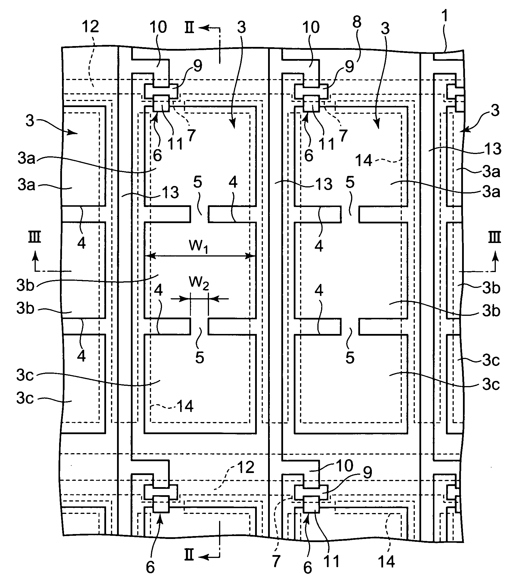
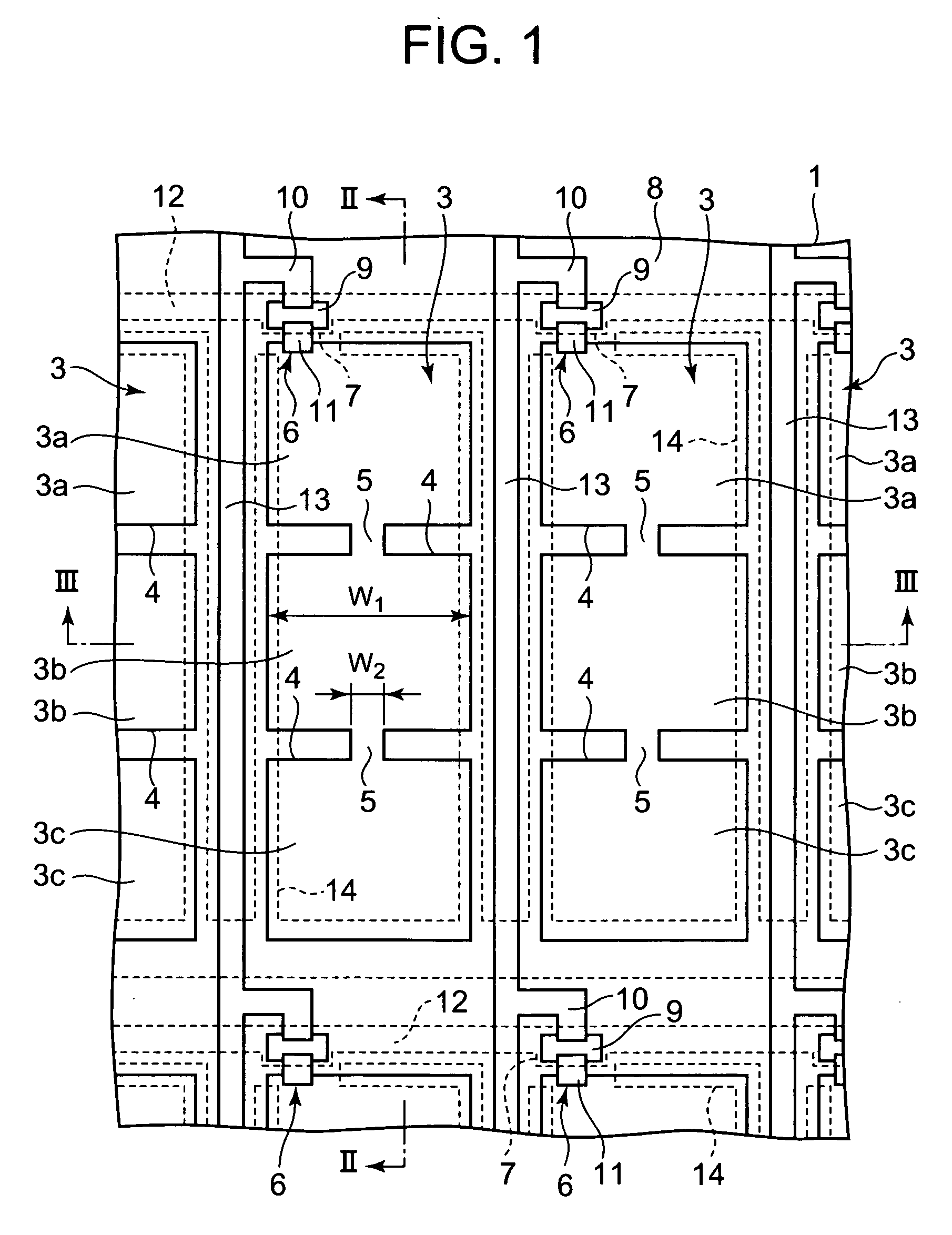
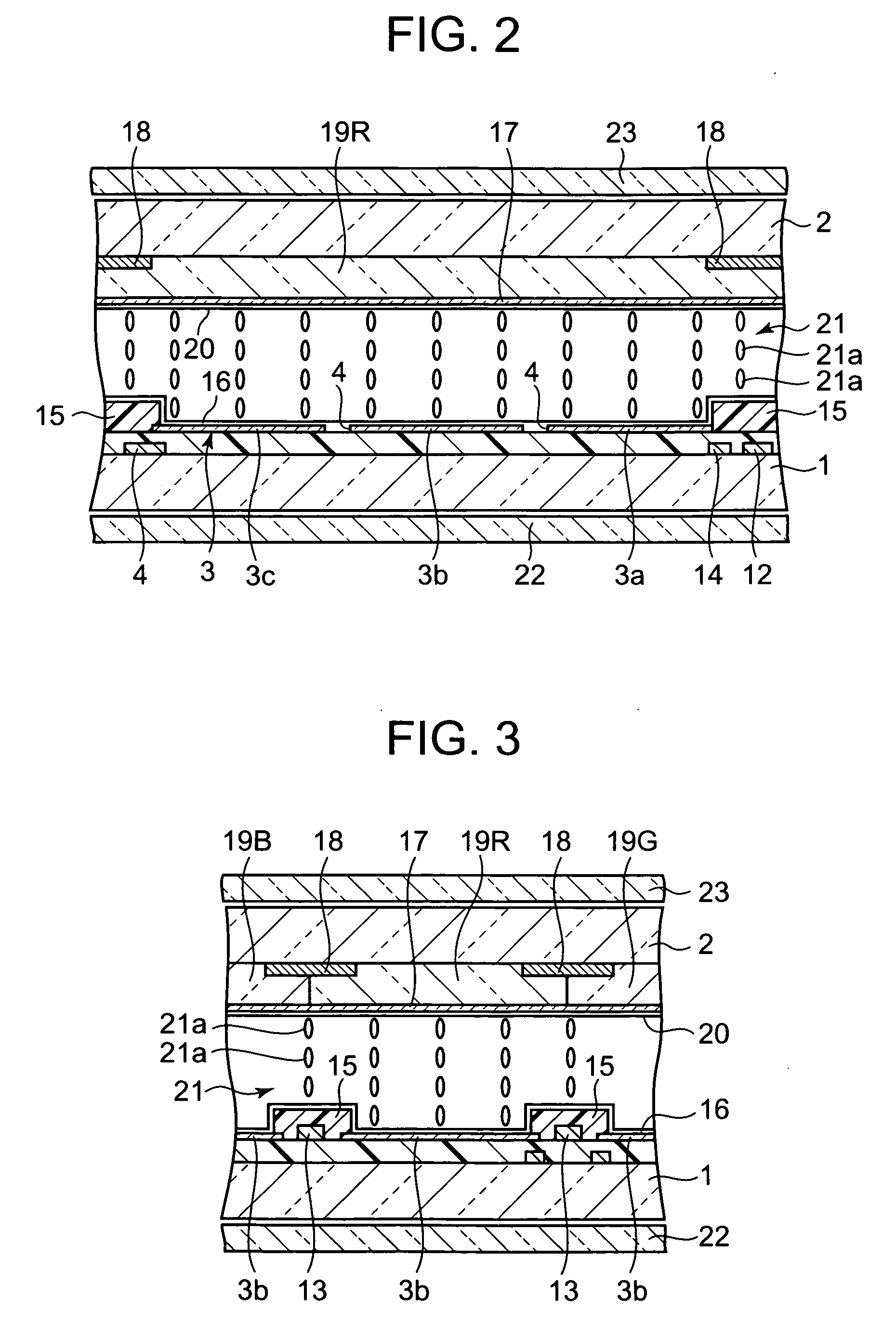
[0063]FIG. 1 to FIG. 4 show the first embodiment of the present invention, where FIG. 1 is a plan view of a liquid crystal display device showing one part of a substrate on which pixel electrodes are formed, and FIG. 2 and FIG. 3 are cross sections of the liquid crystal display device of FIG. 1, as cut along the line II-II and the line III-III respectively.

[0064] The liquid crystal display device is a vertical alignment active matrix liquid crystal display device, and comprises a pair of transparent substrates 1 and 2 opposite to each other with a predetermined gap therebetween as shown in FIG. 1 to FIG. 3. At least one transparent opposing electrode 17 is formed on the inner surface of one substrate of the opposing inner surfaces of the pair of substrates 1 and 2, for example, on the inner surface of the substrate 2 on the viewer side (hereinafter referred to as front substrate). Formed on the inner surface of the other substrate of the opposing inner surfaces of the pair of subst...

second embodiment

[0089]FIG. 5 is a plan view of one part of one substrate of a liquid crystal display device as the second embodiment of the present invention. In the present embodiment, the components same as those in the first embodiment will be given the same reference numerals, and explanation for such components will be omitted.

[0090] The liquid crystal display device according to the present embodiment is structured as follows: the plurality of pixel electrodes 3 are formed in an elongated shape having shorter sides in the row direction and longer sides in the column direction; the source electrode 11 of each TFT 6 is connected to one end of one shorter side of each of the plurality of pixel electrodes 3; the pixel electrodes 3 are each provided with slits 41 which separate the pixel electrode 3 into a plurality of, for example, three electrode portions 3a, 3b, and 3c which are arranged side by side in the direction of the longer side; and connecting portions 51 at which the electrode portion...

third embodiment

[0101]FIG. 7 is a plan view of one pixel on one substrate of a liquid crystal display device as the third embodiment of the present invention. In the present embodiment, the components same as those in the first and second embodiments will be given the same reference numerals, and explanation for such components will be omitted.

[0102] The liquid crystal display device according to the present embodiment is structured as follows; the pixel electrode 3 having an elongated shape is provided with a plurality of slits 42 which separate the pixel electrode 3 into three or more (three according to the present embodiment) electrode portions 3a, 3b, and 3c which are arranged side by side in the direction of the longer side of the pixel electrode 3; a connecting portion 52 at which, of the electrode portions 3a, 3b, and 3c of the pixel electrode 3, the electrode portion 3a to which the TFT 6 is connected and the electrode portion 3b adjoining the electrode portion 3a are connected with each ...


PUM

PropertyMeasurementUnit
Widthaaaaaaaaaa
Dielectric anisotropyaaaaaaaaaa
Shapeaaaaaaaaaa

Abstract

A liquid crystal display device has an opposing substrate on which an opposing electrode is formed, a TFT substrate on which pixel electrodes arranged in matrix, thin film transistors connected to the pixel electrodes respectively, and gate lines and data lines for the thin film transistors are formed, vertical alignment films formed on the opposing inner surfaces of these substrates, and a liquid crystal layer disposed between the vertical alignment films and having negative dielectric anisotropy. Each pixel electrode has a slit formed for separating each pixel into a plurality of sub-pixels by partially eliminating the pixel electrode with a connecting portion left at which adjoining electrode portions of each pixel electrode is connected with each other. The width W1 of the pixel electrode that runs in a direction in which the slit is formed and width W2 of the connecting portion have a ratio W2 / W1 of 0.13 or lower.

Description

BACKGROUND OF THE INVENTION [0001] 1. Field of the Invention [0002] The present invention relates to a vertical alignment active matrix liquid crystal display device using a thin film transistor (hereinafter referred to as TFT) as an active element. [0003] 2. Description of the Related Art [0004] A vertical alignment liquid crystal display device comprises a pair of substrates opposite to each other with a predetermined gap therebetween, a plurality of pixel electrodes arranged in a matrix of rows and columns on the inner surface of one substrate of the opposing inner surfaces of the pair of substrate, a plurality of TFTs arranged on the inner surface of the one substrate correspondingly to the plurality of pixel electrodes and connected to the corresponding pixel electrodes, a plurality of gate lines and data lines formed on the inner surface of the one substrate respectively between the rows of pixel electrodes and the columns of pixel electrodes for supplying a gate signal and a ...

Claims


Application Information

Patent Timeline
IPC IPC(8): G02F1/1337
CPCG02F1/133707G02F1/133711G02F1/1343G02F1/1393G02F2001/133742G02F2001/13712G02F2201/122G02F1/133742G02F1/13712G02F1/1337
Inventor YAMAGUCHI, MINORUNAKAJIMA, YASUSHIMIZUSAKO, RYOTA
Owner ORTUS TECH
Why Eureka
Try Eureka