Method for manufacturing a semconductor device

a manufacturing method and semiconductor technology, applied in the direction of semiconductor devices, basic electric elements, electrical equipment, etc., can solve the problems of difficult to achieve mask alignment in the subsequent process, poor electrical properties of the semiconductor layer, etc., and achieve the effect of high performan

Inactive Publication Date: 2006-06-08
SEMICON ENERGY LAB CO LTD
View PDF48 Cites 3 Cited by
  • Summary
  • Abstract
  • Description
  • Claims
  • Application Information

AI Technical Summary

Benefits of technology

[0005] It is an object of the present invention to provide a method for manufacturing a semiconductor device of high performance.
[0006] It is another object of the present invention to provide a semiconductor device comprising a channel region of high field effect mobility.
[0007] It is a further object of the present invention to provide a semiconductor device of high performance.
[0008] In order to attain these and other objects, first a glass substrate is heated in a non-oxidizing atmosphere or an inactive gas atmosphere at a temperature not higher than strain point of the glass substrate, and then a non-single crystal semiconductor layer is formed on the substrate and the non-single crystal semiconductor layer is crystallized by heat in a non-oxidizing atmosphere or an inactive gas atmosphere. The volume of the glass substrate at a temperature, e.g., room temperature after the glass substrate heating process is smaller than that at the same temperature as the above, e.g., room temperature before the glass substrate heating process. That is, the glass substrate shrinks after being heated. By virtue of this glass substrate heating process, when the non-single crystal semiconductor layer formed on the glass substrate is crystallized by heat, the volume of the glass substrate is not decreased so much, that is, the shrink of the glass substrate is very little. Therefore, a crystallized semiconductor layer free from internal stress can be obtained by the crystallization process.

Problems solved by technology

Further, photolithography pattern to be used in the subsequent process is deformed due to the shrink of the glass substrate, so that mask alignment in the further subsequent process becomes difficult to carry out.
According to an experiment, interface state in the semiconductor layer formed on the substrate was high due to the internal stress, therefore electrical property of the semiconductor layer was bad.

Method used


Image

  • Method for manufacturing a semconductor device
  • Method for manufacturing a semconductor device
  • Method for manufacturing a semconductor device

Examples


first embodiment

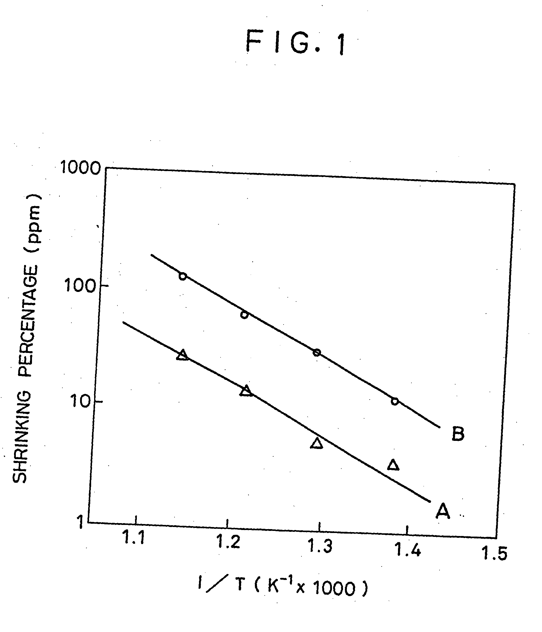
[0035] Glass substrates A (AN-2 non-alkali glass) which had been heated in advance in the same manner as in the first embodiment were prepared. Also, glass substrates B (AN-2 non-alkali glass) which had never been heated were prepared. First, volume of each substrate was measured at room temperature (the volume obtained is referred to as V1). Then these glass substrates were heated at various temperatures for 12 hours. After the heating process, volume of each substrate was measured again at room temperature (the volume obtained is referred to as V2). Then, shrinking percentage of each substrate was calculated by the volume V1 and the volume V2 of each substrate. Relationship between the shrinking percentages of the heated glass substrates A and the temperatures is shown by line A in FIG. 1, while that in the case of the glass substrates B is shown by line B. As apparent from FIG. 1, the shrinking percentages of the glass substrates A heated in advance are ⅕ or less of those of the ...

second embodiment

[0042] Referring next to FIGS. 4(A) through 4(E), manufacture of a polycrystal silicon thin film transistor will be described in accordance with the present invention.

[0043] A glass substrate (AN-2 non-alkali glass) 1 was heated at 610° C. for 12 hours in an electrical furnace. This heating was carried out in an inactive gas atmosphere, e.g. N2, under an atmospheric pressure. It may be done in an inactive gas atmosphere involving an additive of hydrogen under an atmospheric pressure or a reduced pressure, instead.

[0044] On the glass substrate 1, a silicon compound layer 2, e.g. SiO2 layer, was formed to be 200 nm thick by RF sputtering method. The formation was carried out under conditions of a pressure of 0.5 Pa, a temperature of 100° C., an RF frequency of 13.56 MHz, and an RF output power of 400 W.

[0045] Then, an amorphous silicon activation layer 3 was formed to be 100 nm thick on the silicon compound layer by RF sputtering. In this case, the formation was carried out under a ...

third embodiment

[0053] In accordance with the present invention, formation of a semiconductor layer on a substrate will be described hereinafter.

[0054] An AN-2 non-alkali glass whose strain point is 616° C., was utilized as a substrate. This glass substrate was heated at 610° C. for 12 hours in an electrical furnace. This heating process was carried out in an inactive gas atmosphere, e.g. N2, involving hydrogen at 50% under an atmospheric pressure. Then a silicon compound layer, e.g. SiO2 layer, was formed to be 200 nm thick by magnetron RF sputtering, and subsequently an amorphous silicon layer was formed thereon to be 100 nm thick by means of a magnetron RF sputtering apparatus in an atmosphere of a hydrogen partial pressure of 0.75 mTorr and an argon partial pressure of 3.00 mTorr at an RF power of 400 W, utilizing a target made of silicon. Then the amorphous silicon layer was crystallized by heat at 600° C. for 96 hours.

[0055] Shrinking percentages of glass substrates D which had been heated i...


PUM

PropertyMeasurementUnit
temperatureaaaaaaaaaa
strain pointaaaaaaaaaa
viscosityaaaaaaaaaa

Abstract

A semiconductor device is manufactured by the use of a glass substrate which has previously been heated. An amorphous semiconductor layer is formed on the previously heated glass substrate and then crystallized by heat. By virtue of the previous heating, shrink of the glass substrate after the crystallization process is reduced. Accordingly, internal stress is not generated in the crystallized semiconductor layer. The semiconductor device thus manufactured is superior in electrical property.

Description

BACKGROUND OF THE INVENTION [0001] 1. Field of the Invention [0002] The present invention relates to a method for manufacturing a semiconductor device. [0003] 2. Description of the Prior Art [0004] A technique of forming a non-single crystal semiconductor layer on a glass substrate by reduced pressure CVD or plasma CVD followed by heating the substrate at about 600° C. to thereby crystallize the layer into a polycrystal semiconductor layer has been well-known in the field of manufacture of semiconductor devices. Explaining the process of this thermal crystallization, first the temperature is raised from room temperature (i.e. initial stage), second the temperature is maintained at about 600° C. (i.e. intermediate stage) for a few hours to several tens hours, and finally the temperature is lowered to room temperature (i.e. last stage). If a cheap glass substrate utilized for a large-sized liquid crystal display device and so on is subjected to the thermal crystallization process at a...

Claims


Application Information

Patent Timeline
Patent Type & Authority Applications(United States)
IPC IPC(8): H01L21/84H01L21/20H01L21/336H01L21/77
CPCH01L21/2022H01L27/1285H01L29/78603H01L29/66757H01L21/0262H01L21/02667H01L21/02576H01L21/02422H01L21/02488H01L21/02502H01L21/02496H01L21/02532H01L21/0245H01L21/02631
Inventor ZHANG, HONGYONG
Owner SEMICON ENERGY LAB CO LTD
Why Eureka
Try Eureka