
Contact for dual liner product

a dual-liner, contact technology, applied in the direction of semiconductor devices, semiconductor/solid-state device details, electrical equipment, etc., can solve the problems of contact open failure, contact open failure, certain problems,

Active Publication Date: 2006-05-11
GLOBALFOUNDRIES US INC
View PDF4 Cites 37 Cited by
  • Summary
  • Abstract
  • Description
  • Claims
  • Application Information

AI Technical Summary

Benefits of technology

[0002] In fabricating integrated circuits in conventional bulk semiconductor wafers, wells of either p-type or n-type conductivity are implanted in a substrate of the opposite conductivity. However, in complementary metal oxide semiconductor (CMOS) technology, both p-type and n-type wells are utilized. Source / drain regions are formed by implanting diffusion regions of the opposite n-type or p-type conductivity as the wells to form metal-oxide-semiconductor field effect transistors (MOSFETs). Recent theoretical and empirical studies have also demonstrated that carrier mobility in a transistor can be increased when a stress of sufficient magnitude is applied to the conduction channel of a transistor to create a strain therein. An increase in the performance of an n-type field effect transistor (NFET) can be achieved by applying a tensile longitudinal stress to the conduction channel of the NFET. An increase in the performance of a p-type field effect transistor (PFET) can be achieved by applying a compressive longitudinal stress to the conduction channel of the PFET.
[0003] A stress-imparting film, also referred to herein as a “stressed” film, can be deposited to cover a semiconductor device region to impart a stress thereto for enhancing the conductivity of a transistor, for example, an NFET or a PFET device. Silicon nitride is one material, among others, which can be deposited in such way that the resulting material layer imparts either a tensile stress or a compressive stress to a layer of a second material with which it is in contact. To improve the conductivity of both an NFET and a PFET, a tensile stress-imparting nitride can be formed to cover an NFET device region and a compressive stress-imparting nitride can be formed to cover a PFET device region.

Problems solved by technology

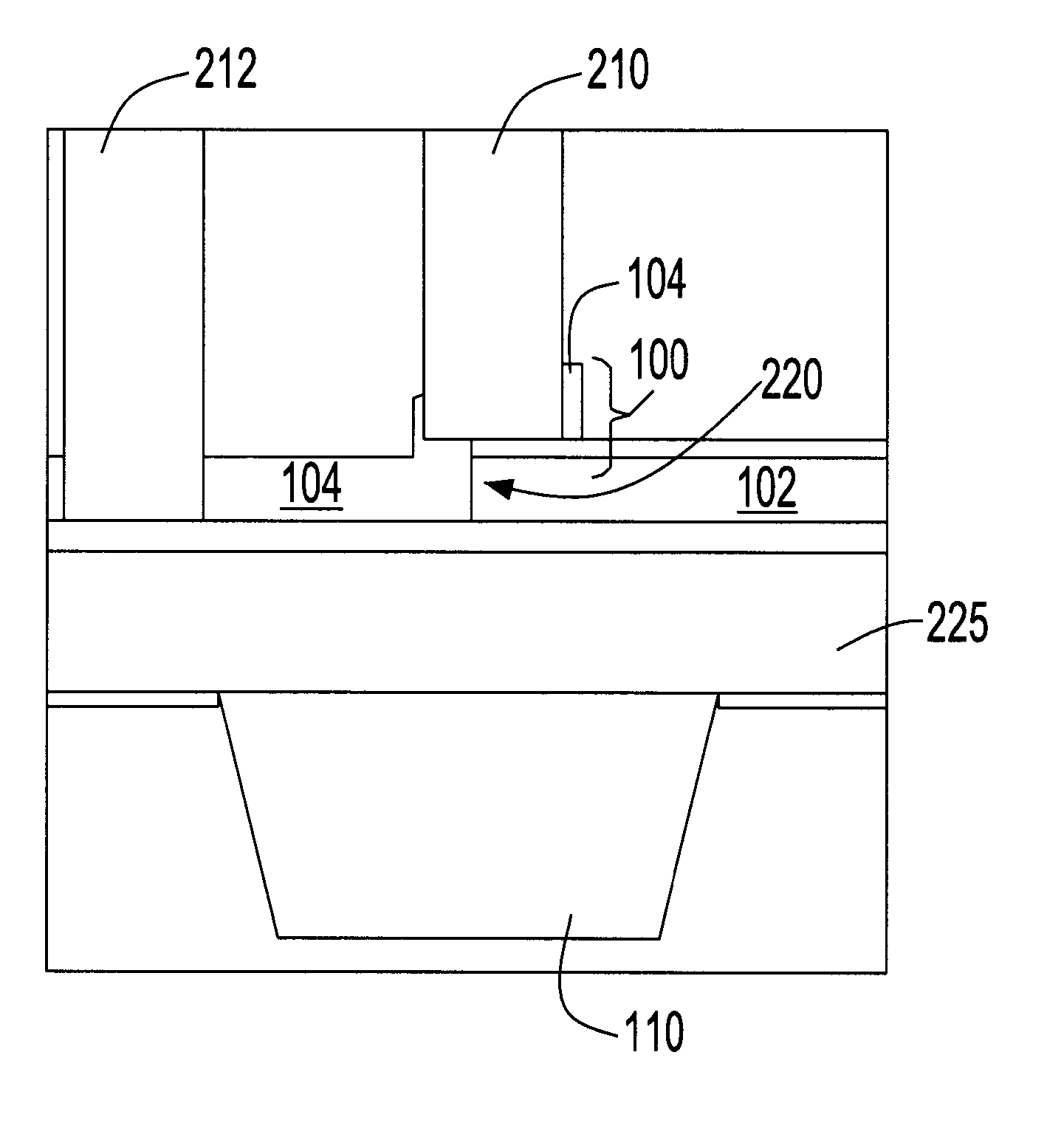
An overlapped boundary, however, can create certain problems.
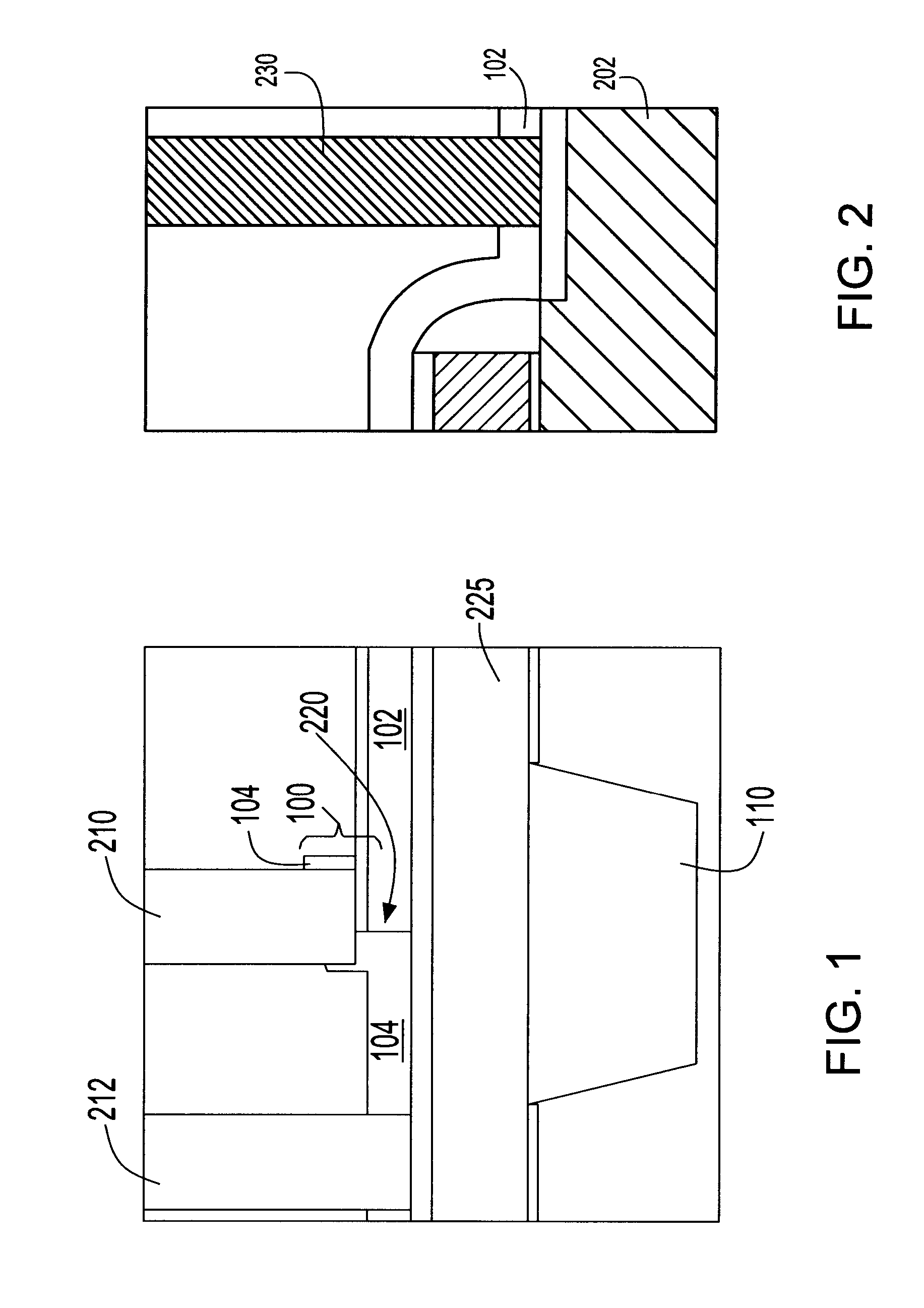
Indeed, a contact open failure can result, as best seen at 220 in FIG. 1.
A contact open failure can occur when the contact hole fails to be etched sufficiently.

Method used


Image

  • Contact for dual liner product
  • Contact for dual liner product
  • Contact for dual liner product

Examples


Embodiment Construction

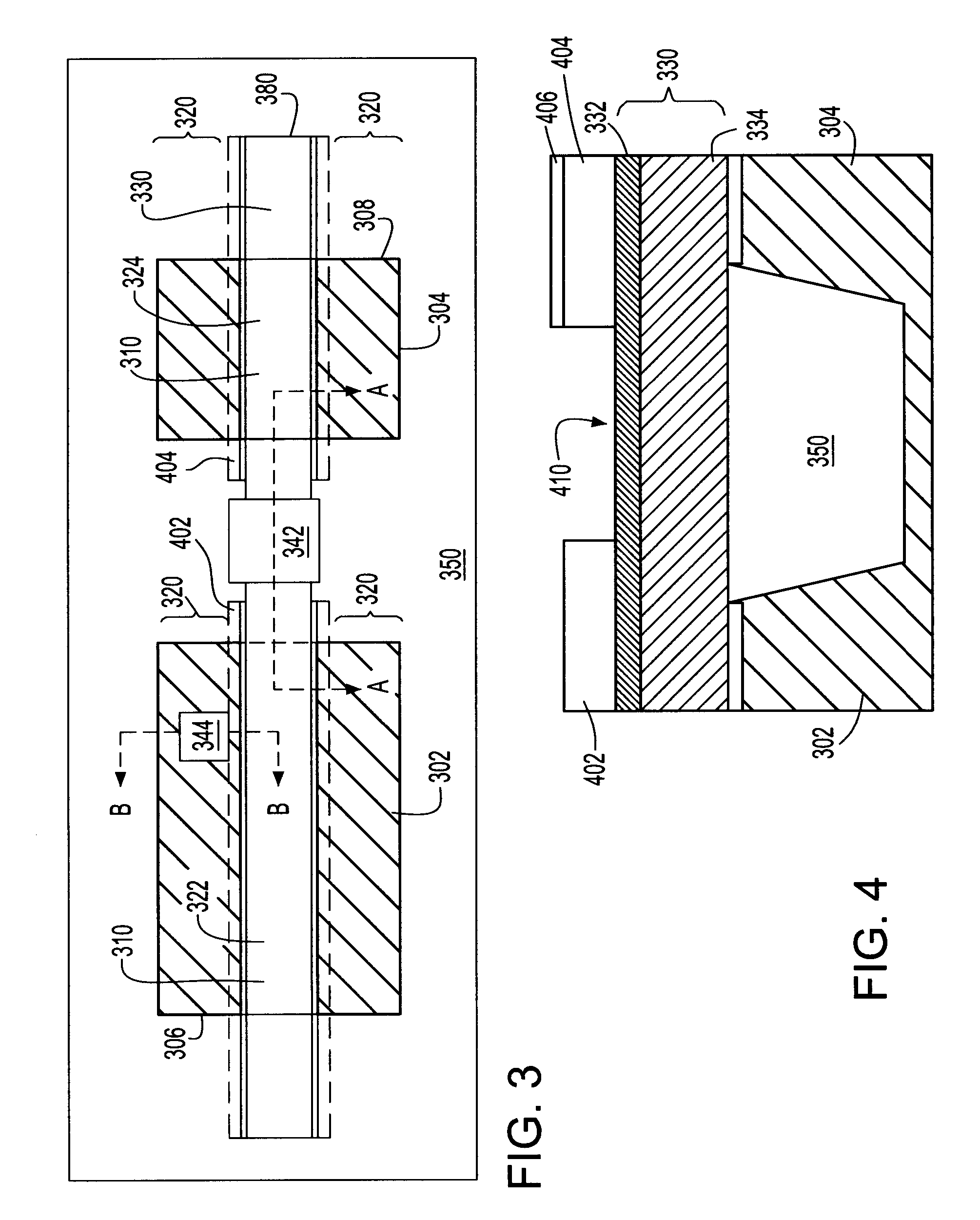
[0013] Although an underlapped structure accomplishes the goals of providing dual stress imparting films over the NFET and the PFET and reduces the etching concerns in overlapped boundaries, it does not resolve all of the etching concerns discussed earlier. One potential way of addressing the etching problem is to reduce the thickness of or eliminate films to be etched, and add structure which retards etching process. Such solution will now be described with reference toFIGS. 3 through 10.

[0014]FIG. 3 is a top-down view illustrating an embodiment of the present invention. As illustrated in FIG. 3, semiconductor device regions 302, 304 are provided in a semiconductor substrate. In the embodiment of FIG. 3, the semiconductor device regions 302, 304 are isolated by a shallow trench isolation 350, which surrounds them. The device regions 302, 304 are processed to form a p-type field effect transistor (PFET) in region 302 and an n-type field effect transistor (NFET) in region 304.

[0015...


PUM


Abstract

A structure is provided which includes a semiconductor device region including a first portion and a second portion. A current-conducting member is provided, which extends horizontally over the first portion but not over the second portion. A first film, such as a stress-imparting film, extends over the second portion and only partially over the current-conducting member to expose a contact portion of the member. A first contact via is provided in conductive communication with the contact portion of the member, the first contact via having a self-aligned silicide-containing region. A second contact via is provided in conductive communication with the second portion of the semiconductor device region, the second contact via extending through the first film.

Description

[0001] The present invention relates to the structure and fabrication of semiconductor devices. [0002] In fabricating integrated circuits in conventional bulk semiconductor wafers, wells of either p-type or n-type conductivity are implanted in a substrate of the opposite conductivity. However, in complementary metal oxide semiconductor (CMOS) technology, both p-type and n-type wells are utilized. Source / drain regions are formed by implanting diffusion regions of the opposite n-type or p-type conductivity as the wells to form metal-oxide-semiconductor field effect transistors (MOSFETs). Recent theoretical and empirical studies have also demonstrated that carrier mobility in a transistor can be increased when a stress of sufficient magnitude is applied to the conduction channel of a transistor to create a strain therein. An increase in the performance of an n-type field effect transistor (NFET) can be achieved by applying a tensile longitudinal stress to the conduction channel of the ...

Claims


Application Information

Patent Timeline
IPC IPC(8): H01L21/4763
CPCH01L21/76816H01L21/76829H01L21/76834H01L21/76847H01L21/76867H01L21/76897H01L21/823807H01L2924/0002H01L21/823871H01L23/485H01L29/7842H01L29/7843H01L2924/00H01L21/28518H01L21/76805H01L21/76832H01L21/76843H01L21/76855
Inventor YANG, HAINING S.WANN, CLEMENT H.ZHU, HUILONG
Owner GLOBALFOUNDRIES US INC
Learn More