
Thermally conductive emi shield

a technology of emi shield and thermal conductor, applied in the field of thermal management, to achieve the effect of reducing the transmission of emi

Active Publication Date: 2006-05-11
LAIRD TECH INC
View PDF8 Cites 44 Cited by
  • Summary
  • Abstract
  • Description
  • Claims
  • Application Information

AI Technical Summary

Benefits of technology

[0009] In general, the present invention relates to an electromagnetic-interference-absorbing thermally-conductive gap filler, such as an elastomeric (for example, silicone) pad treated with an electromagnetic-interference-absorbing material. The EMI-absorbing material absorbs a portion of the EMI incident upon the treated thermal pad, thereby reducing transmission of EMI therethrough over a range of operational frequencies. The absorbing material may remove a portion of the EMI from the environment through power dissipation resulting from loss mechanisms. These loss mechanisms include polarization losses in a dielectric material and conductive, or ohmic, losses in a conductive material having a finite conductivity.
[0010] Accordingly, in a first aspect, the invention relates to a composite material for reducing electromagnetic emissions generated by an electronic device, the composite material including, in combination, a thermally conductive material and an electromagnetic-energy-absorptive material. The thermally conductive material facilitates transfer of thermal energy from the device and the electromagnetic-energy-absorptive material reduces electromagnetic emissions generated by the device.

Problems solved by technology

The absorbing material may remove a portion of the EMI from the environment through power dissipation resulting from loss mechanisms.

Method used


Image

  • Thermally conductive emi shield
  • Thermally conductive emi shield
  • Thermally conductive emi shield

Examples


Embodiment Construction

[0027] Materials having electromagnetic-energy absorbing properties can be used to suppress the transmission of EMI over a broad range of frequencies. Such EMI-absorbing materials can provide substantial electromagnetic-shielding effectiveness, for example, up to about 5 dB or more at EMI frequencies occurring from about 2 GHz up to about 100 GHz.

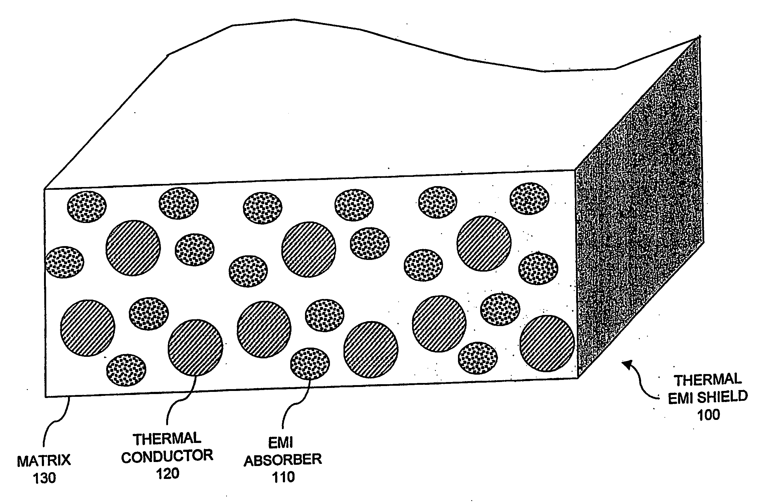
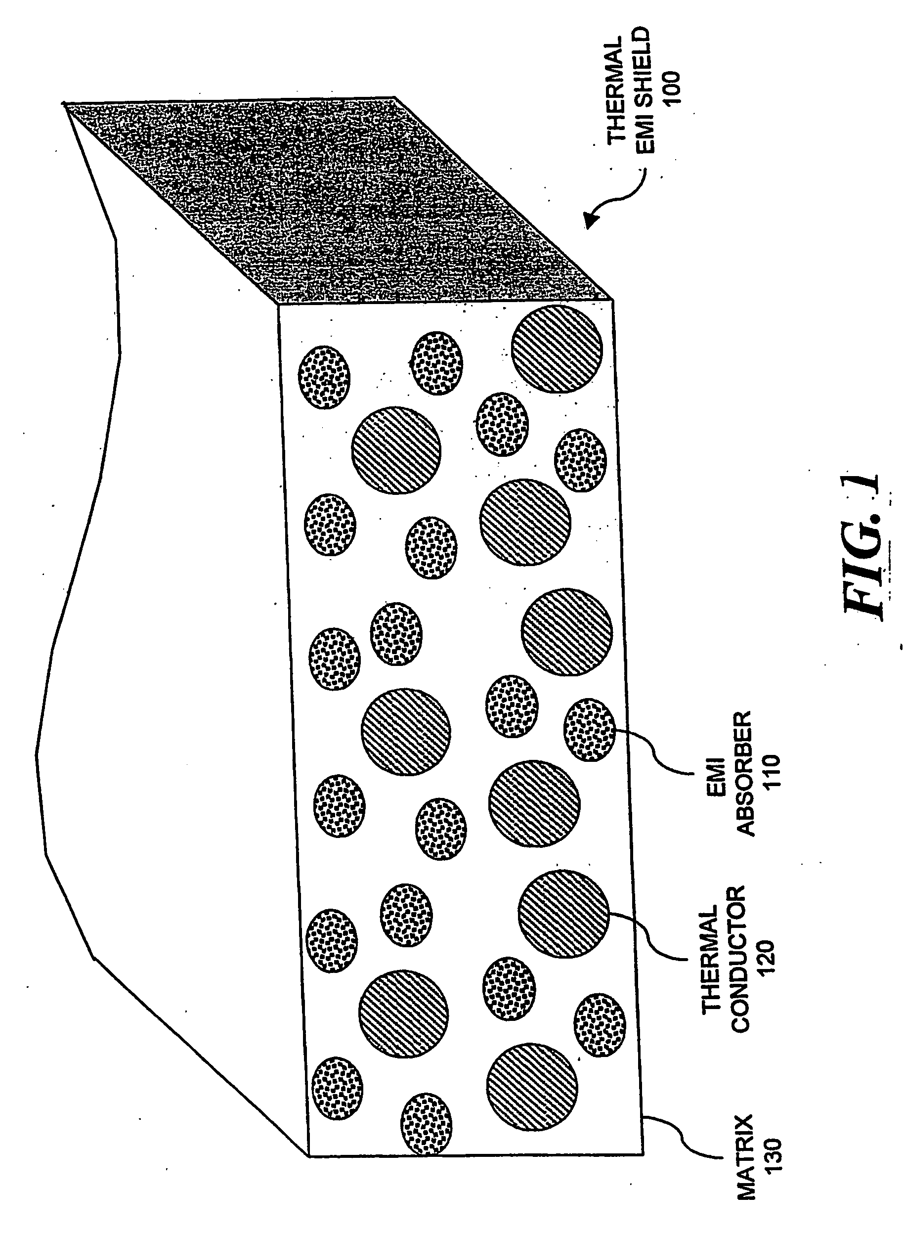
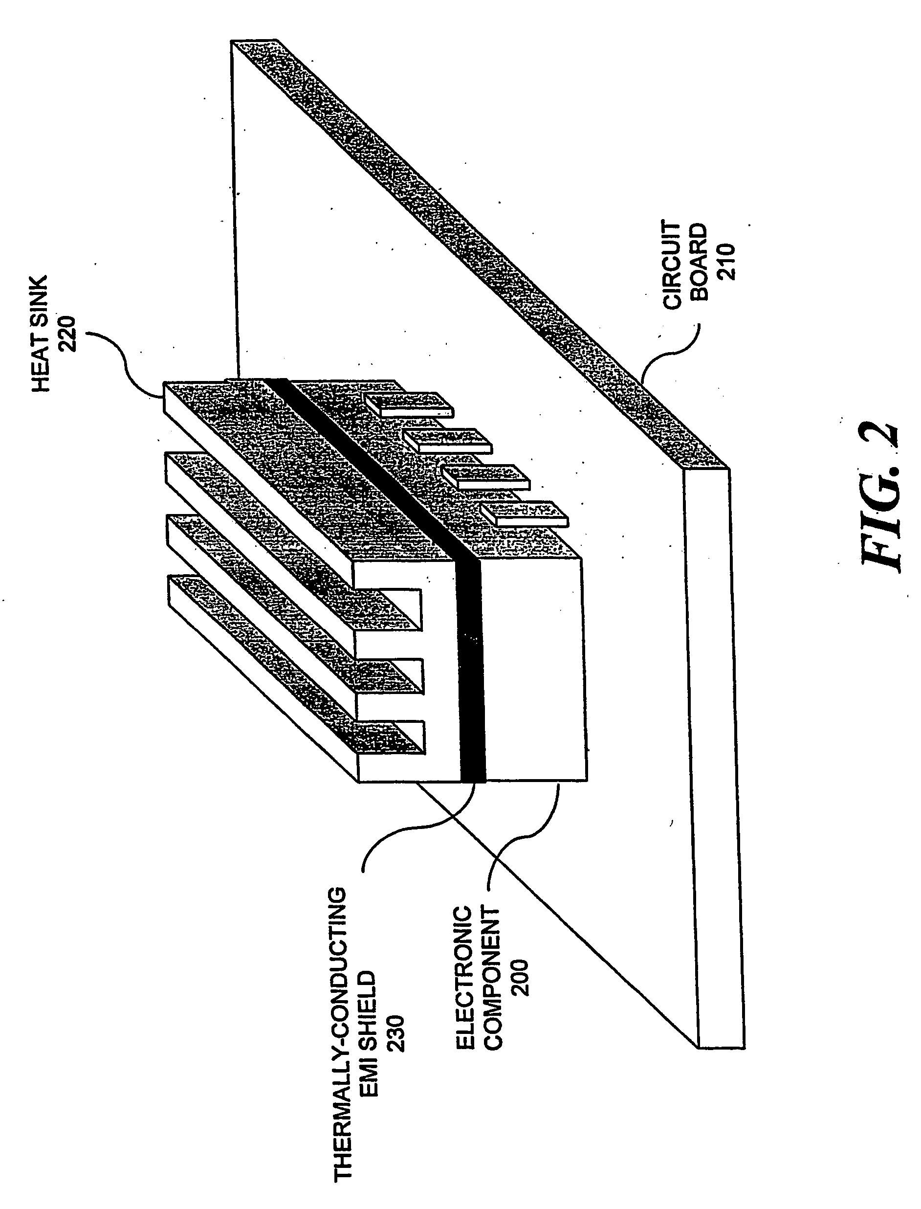
[0028] According to the present invention, a thermally-conductive EMI absorber can be formed by combining EMI-absorbing fillers and thermally conducting fillers in a base matrix (for example, an elastomer) capable of being applied as a thermal gap filler, or pad. Generally, the resulting thermally-conductive EMI absorber can be applied as any thermal conductive material, for example, as between an electronic component (e.g., a “chip”) and a heat sink.

[0029] Referring to FIG. 1, a thermally-conductive EMI absorber (thermal EMI shield) 100 is illustrated as a rectangular volume. The front face of the thermal EMI shield 100 represents a cros...


PUM

PropertyMeasurementUnit
dielectric constantaaaaaaaaaa
thicknessaaaaaaaaaa

Abstract

Electromagnetic-energy absorbing materials are combined with thermally conductive materials, such as those used for thermal management in association with electronic equipment, thereby suppressing the transmission of electromagnetic interference (EMI) therethrough. Disclosed are materials and processes for combining EMI-absorbing materials with thermally conductive materials thereby improving EMI shielding effectiveness in an economically efficient manner. In one embodiment, a thermally conductive EMI absorber is prepared by combining an EMI-absorbing material (for example, ferrite particles) with a thermally conducting material (for example, ceramic particles), each suspended within an elastomeric matrix (for example, silicone). In application, a layer of thermally conductive EMI-absorbing material is applied between an electronic device or component, and a heat sink

Description

BACKGROUND OF THE INVENTION [0001] 1. Field of the Invention [0002] The present invention relates generally to thermal management in electronic applications and, more specifically, to thermal conductors incorporating electromagnetic-energy-attenuating properties. [0003] 2. Description of the Prior Art [0004] As used herein, the term EMI should be considered to refer generally to both electromagnetic interference and radio-frequency-interference (RFI) emissions, and the term “electromagnetic” should be considered to refer generally to electromagnetic and radio frequency. [0005] Electronic devices typically generate thermal emissions as an unavoidable byproduct. The amount of thermal emissions generated can correlate to the switching speed and complexity of the source electronic component or device. As newer electronic devices tend to operate at greater and greater switching speeds, they will also result in greater thermal emissions. These increased thermal emissions, at some level, p...

Claims


Application Information

Patent Timeline
Patent Type & Authority Applications(United States)
IPC IPC(8): B32B15/00G11B11/105B05D5/12B32B9/00H01L23/373H01L23/552H05K7/20H05K9/00
CPCH01L23/3733Y10T428/25H01L23/552H01L2224/73253H01L2924/16152H01L2924/3011H05K7/20481H05K9/0083H01L2924/01055H01L2924/01068H01L23/3737Y10T428/32H01L2224/32245Y10T428/26Y10T428/256Y10T428/257Y10T428/31855Y10T428/31801Y10T428/31551
Inventor JOHNSON, RICHARD NORMAN
Owner LAIRD TECH INC
Learn More