
Apparatus and method for enhanced transient blocking

a technology of enhanced transient blocking and apparatus, applied in the direction of pulse technique, transistor, electronic switching, etc., can solve the problems of frequent insufficient performance parameters of fuses and protection circuits, limited performance, and permanent damage, so as to reduce the total resistance of an apparatus, reduce power loss, and increase system efficiency

Active Publication Date: 2006-05-11
BOURNS INC
View PDF31 Cites 32 Cited by
  • Summary
  • Abstract
  • Description
  • Claims
  • Application Information

AI Technical Summary

Benefits of technology

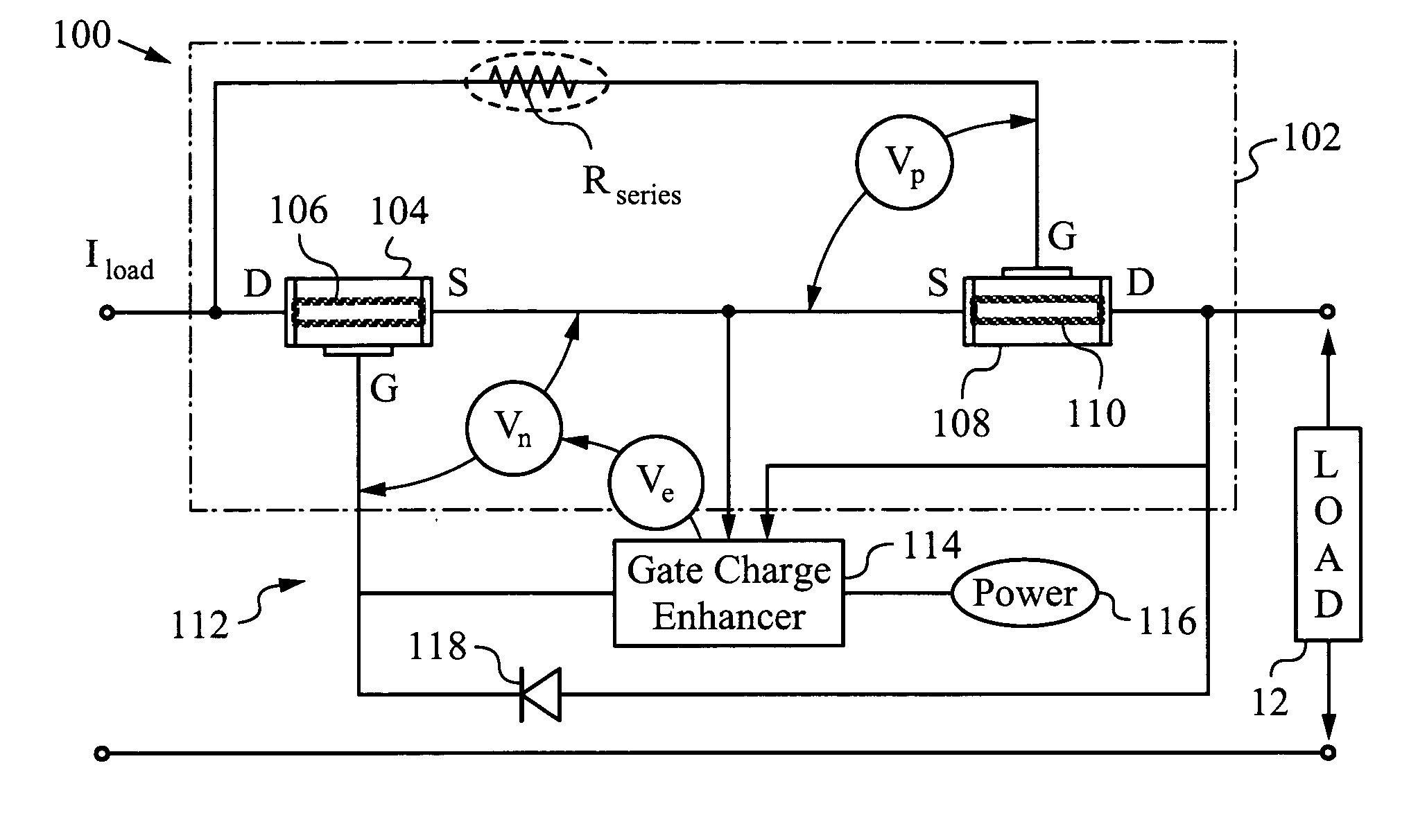
[0008] In view of the above prior art limitations, it is an object of the invention to provide an apparatus and method to permit transient blocking at low voltage drops and currents to reduce power loss and increase system efficiency. In particular, it is an object of the invention to reduce the total resistance of an apparatus that blocks transients.
[0009] It is another object of the invention to ensure that the apparatus is easy to make, low-cost and highly integrable, e.g., on the same die with a traditional transient blocking unit (TBU).
[0010] These and other objects and advantages of the invention will become apparent from the ensuing description.
[0011] The objects and advantages of the invention are addressed by an apparatus for enhanced transient blocking. The apparatus has a transient blocking unit (TBU) that uses at least one depletion mode n-channel device interconnected with at least one depletion mode p-channel device. The interconnection is performed such that a transient alters a bias voltage Vp of the p-channel device and a bias voltage Vn of the n-channel device in concert. Specifically, the bias voltages are altered such that the p-channel device and n-channel device mutually switch off to block the transient. The depletion mode n-channel device used by the TBU can be a junction-gate field effect transistor (JFET) or a metal-oxide-silicon field effect transistor (MOSFET). The apparatus has an enhancer circuit for applying an enhancement bias to a gate terminal of at least one of the depletion mode n-channel devices to reduce a total resistance Rtot of the apparatus.
[0012] In one embodiment, the enhancer circuit comprises a gate charge enhancer. The gate charge enhancer can be connected to an external power source so that the enhancer circuit is powered independently of the TBU. Alternatively, the gate charge enhancer can be connected to the TBU only, such that it draws power through the TBU. In either case, the gate charge enhancer is connected to the TBU for applying the enhancement bias. In one specific embodiment, the gate charge enhancer also has a charge pump. In the same or another embodiment the enhancer circuit has a clamping circuit that may, for example, take advantage of a diode. Specifically, a voltage clamp can be used for limiting a gate-source voltage of the enhancement mode n-channel device of the TBU.
[0013] In still another embodiment of the apparatus of invention, an enhancement mode n-channel MOS (NMOS) transistor is connected to the TBU to reduce the total resistance Rtot. The TBU is connected to a gate terminal of the enhancement mode NMOS. In this embodiment there are two alternatives for powering the TBU. In one case, the TBU is connected to a drain terminal of the enhancement mode NMOS and thus they are commonly powered. In the other case, the transistor and the TBU are separately powered. A gate bias element can be connected to the gate terminal of the enhancement mode NMOS in either of these cases.

Problems solved by technology

Many circuits, networks, electrical devices and data handling systems are operated in configurations and environments where external factors can impair their performance, cause failure or even result in permanent damage.
When providing protection for very sensitive circuits, such as those encountered in telecommunications the performance parameters of the fuses and protection circuits are frequently insufficient.
Unfortunately, when the trigger currents in TBUs are low their performance is limited.
Unfortunately, this is not an option in many high-sensitivity applications.

Method used


Image

  • Apparatus and method for enhanced transient blocking
  • Apparatus and method for enhanced transient blocking
  • Apparatus and method for enhanced transient blocking

Examples


Embodiment Construction

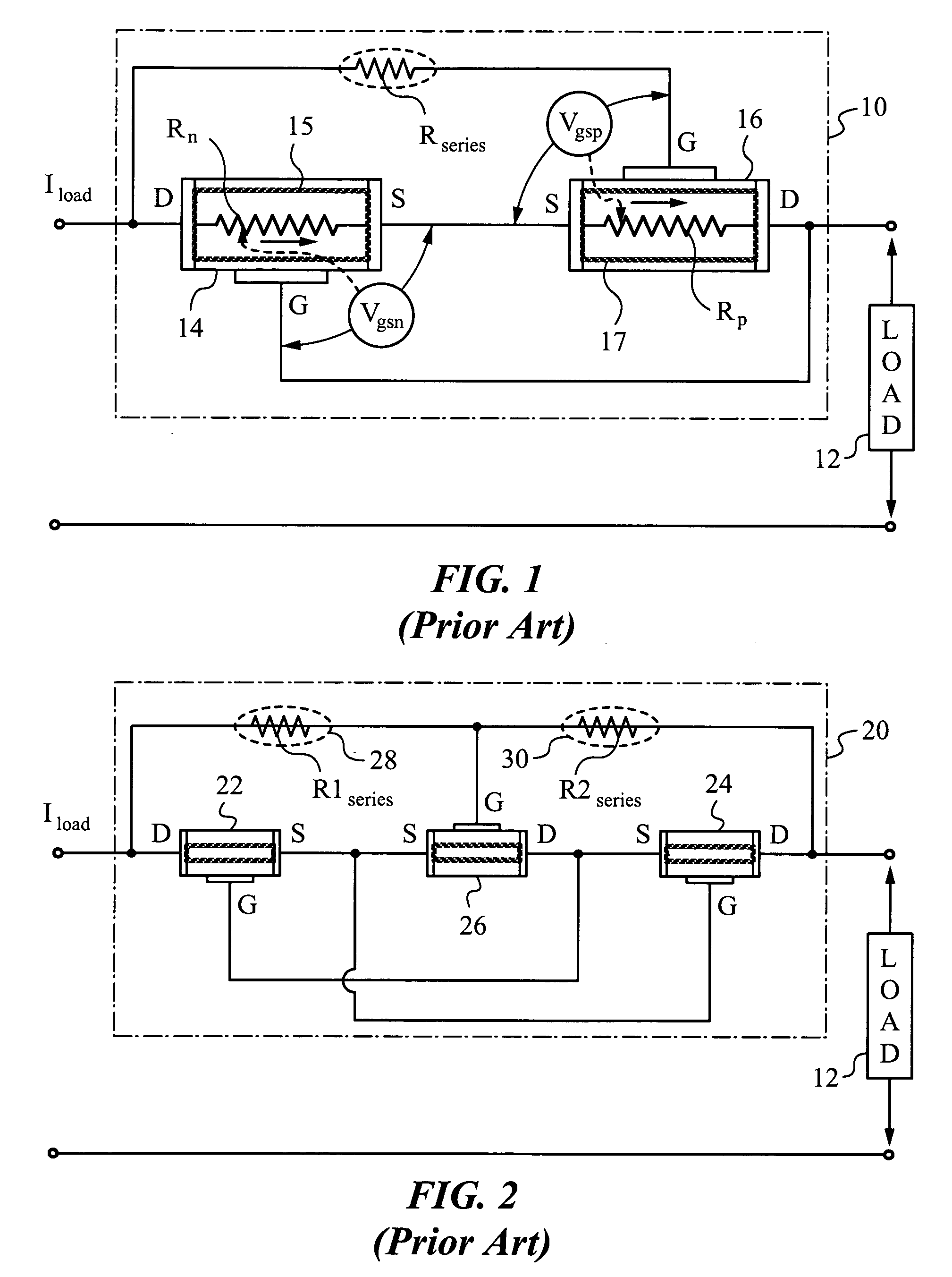
[0027] The present invention and its principles will be best understood by first reviewing prior art uni-directional and bi-directional transient blocking units (TBUs) designed for over-voltage and over-current protection. The diagram in FIG. 1 shows a prior art TBU 10 for protecting a load 12 from voltage and / or current transients of one polarity, i.e., positive voltage spikes or surges. For this reason, TBU 10 is called unidirectional or uni-directional. TBU 10 uses a depletion mode n-channel device 14, typically an n-channel metal-oxide-silicon (NMOS) device implemented as a field effect transistor (FET). TBU 10 also uses a depletion mode p-channel device 16, typically a p-channel junction gate field effect-transistor (PJFET). It should be noted that PMOS, NJFET devices can also be used as devices 14, 16. In the example shown, both NMOS and PJFET 14, 16 are interconnected to take advantage of their n-channel and p-channel biasing and resistance properties to cause mutual switch o...


PUM


Abstract

An apparatus and method for enhanced transient blocking employing a transient blocking unit (TBU) that uses at least one depletion mode n-channel device interconnected with at least one depletion mode p-channel device. The interconnection is performed such that a transient alters a bias voltage Vp of the p-channel device and a bias voltage Vn of the n-channel device such that the p- and n-channel devices mutually switch off to block the transient. The apparatus has an enhancer circuit for applying an enhancement bias to a gate terminal of at least one of the depletion mode n-channel devices of the TBU to reduce a total resistance Rtot of the apparatus. Alternatively, the apparatus has an enhancement mode NMOS transistor and a TBU connected thereto to help provide an enhancement bias to a gate terminal of the enhancement mode NMOS.

Description

RELATED APPLICATIONS [0001] The present application claims the priority from provisional U.S. applications 60 / 626,372; 60 / 626,375 that were co-filed on 9 Nov. 2004 and are herein incorporated in their entirety.FIELD OF THE INVENTION [0002] This invention relates generally to apparatus and methods that employ a transient blocking unit (TBU) in conjunction with an enhancement arrangement to improve performance by reducing resistance and raising current handling capabilities. BACKGROUND ART [0003] Many circuits, networks, electrical devices and data handling systems are operated in configurations and environments where external factors can impair their performance, cause failure or even result in permanent damage. Among the most common of these factors are over-voltage and over-current. Protection against these factors is important and has been addressed in the prior art in a number of ways, depending on the specific electronics and their application. [0004] Fuses that employ thermal o...

Claims


Application Information

Patent Timeline
Patent Type & Authority Applications(United States)
IPC IPC(8): H02H9/00
CPCH01L27/0266H02H5/042H02H5/044H02H9/025H02H9/046
Inventor HARRIS, RICHARD A.HEBERT, FRANCOIS
Owner BOURNS INC
Learn More