Line driver circuit for a semiconductor memory device

a technology of memory device and driver circuit, which is applied in the direction of static storage, digital storage, instruments, etc., can solve the problems of increasing chip size, limited number of memory cells that can be controlled by each word line driver circuit, and increasing chip siz

Inactive Publication Date: 2006-05-04
SAMSUNG ELECTRONICS CO LTD
View PDF12 Cites 17 Cited by
  • Summary
  • Abstract
  • Description
  • Claims
  • Application Information

AI Technical Summary

Benefits of technology

[0024] Each sub word line driver circuit and a corresponding plate line driver circuit may be configured in one unit, and the sub word line driver circuit may include a P-type switch (e.g., PFET transistor) that is driven by the main word line enable signal (and that passes a sub word line enable signal to a selected sub word line); a first N-type switch (e.g., NFET transistor) to prevent floating of sub word line when a main word line disable signal is applied; and a second N-type switch (e.g., NFET transistor) (also driven by the main word line) to prevent floating of sub word line not selected when the main word line enable signal is applied.
[0025] Further, the plate line driver circuit may include a P-type switch (e.g., PFET transistor) that is driven by the main word line (enable signal) and that provides a plate line enable signal to the plate line; and an N-type switch (e.g., NFET transistor) that is also driven by the main word line (disable signal) (to prevent floating of the plate line).

Problems solved by technology

Thus, for driving a large number of memory cells on a chip, a large number of word line driver circuits are required, and the number of memory cells that can be controlled by each word line driver circuit is limited.
As previously noted, the conventional word line driver circuit shown in FIG. 1 is constructed of four transistors (switches) and so in using a large number of word line driver circuits, significant layout area is required on the chip, causing an increase of chip size.
Therefore, in a highly-integrated semiconductor memory device, several word line driver and plate line driver circuits 40 are needed, which occupies significant layout area, causing an increase of chip size.

Method used


Image

  • Line driver circuit for a semiconductor memory device
  • Line driver circuit for a semiconductor memory device
  • Line driver circuit for a semiconductor memory device

Examples


Embodiment Construction

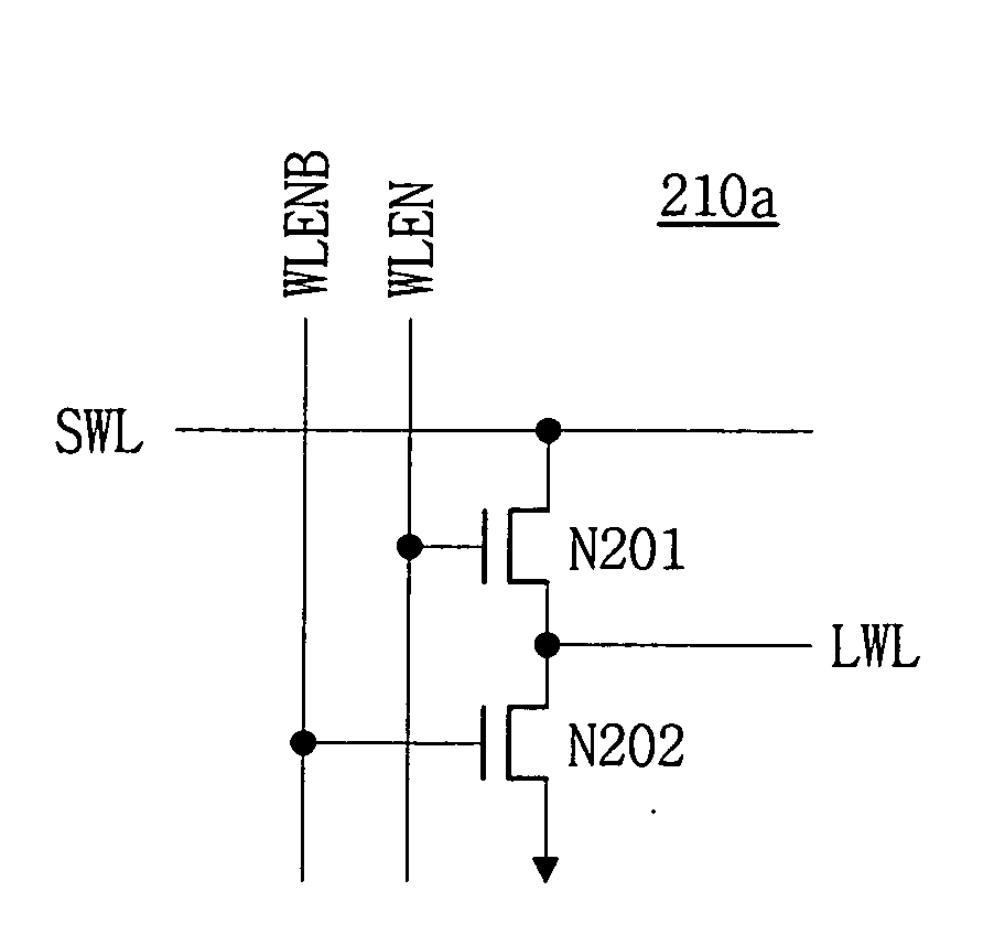
[0042]FIGS. 5 and 11 illustrate a representative part of the layout of a semiconductor memory device according to an embodiment of the invention. In the following description a sub word line will be represented by reference symbol ‘SWL’, a sub word line driver circuit by reference symbol ‘SWD’, a local word line by reference symbol ‘LWL’, and a local word line driver circuit by reference symbol ‘LWD’.

[0043]FIG. 5 is a block diagram illustrating the layout of word line driver circuits in a semiconductor memory device according to an exemplary embodiment of the invention.

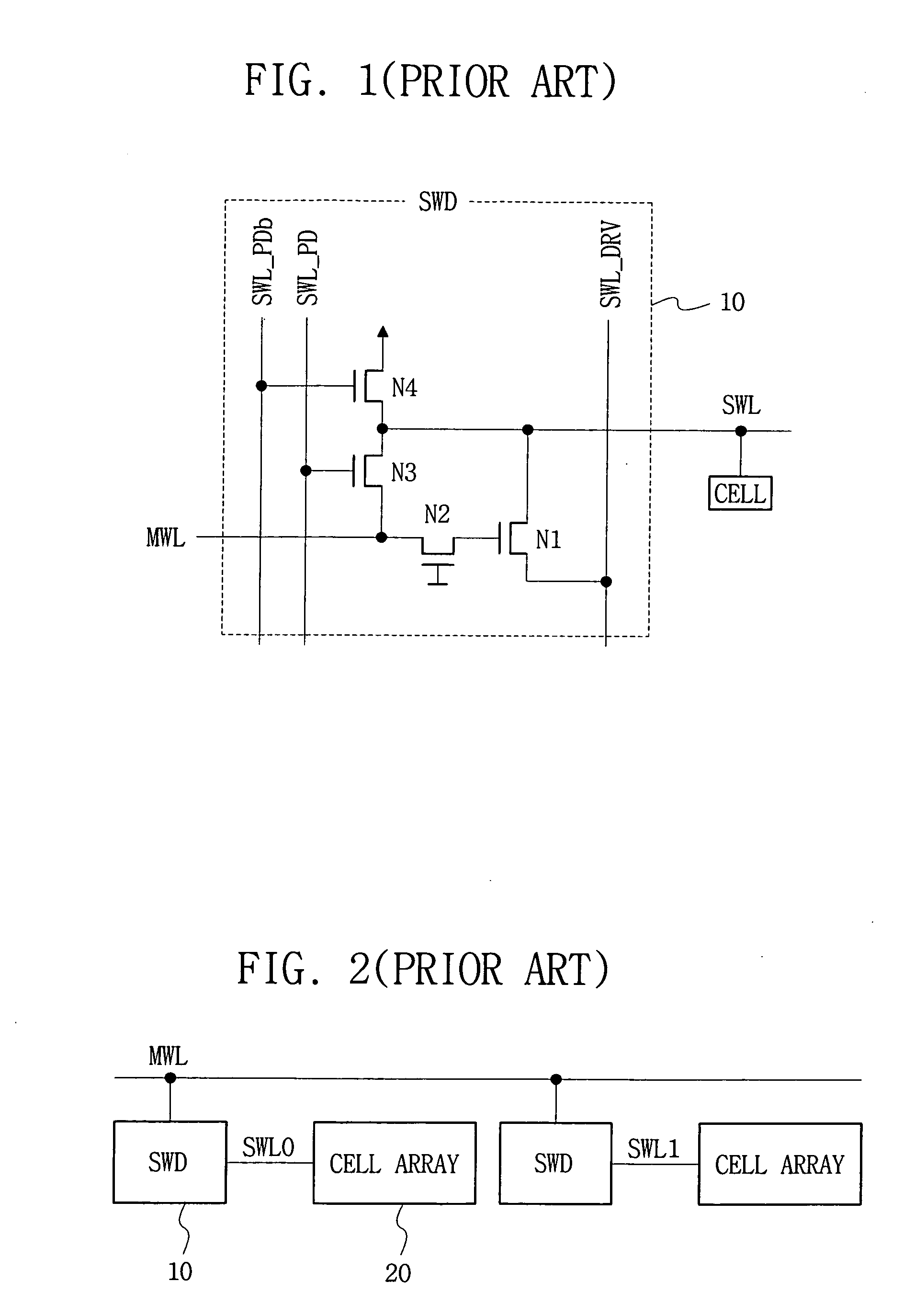
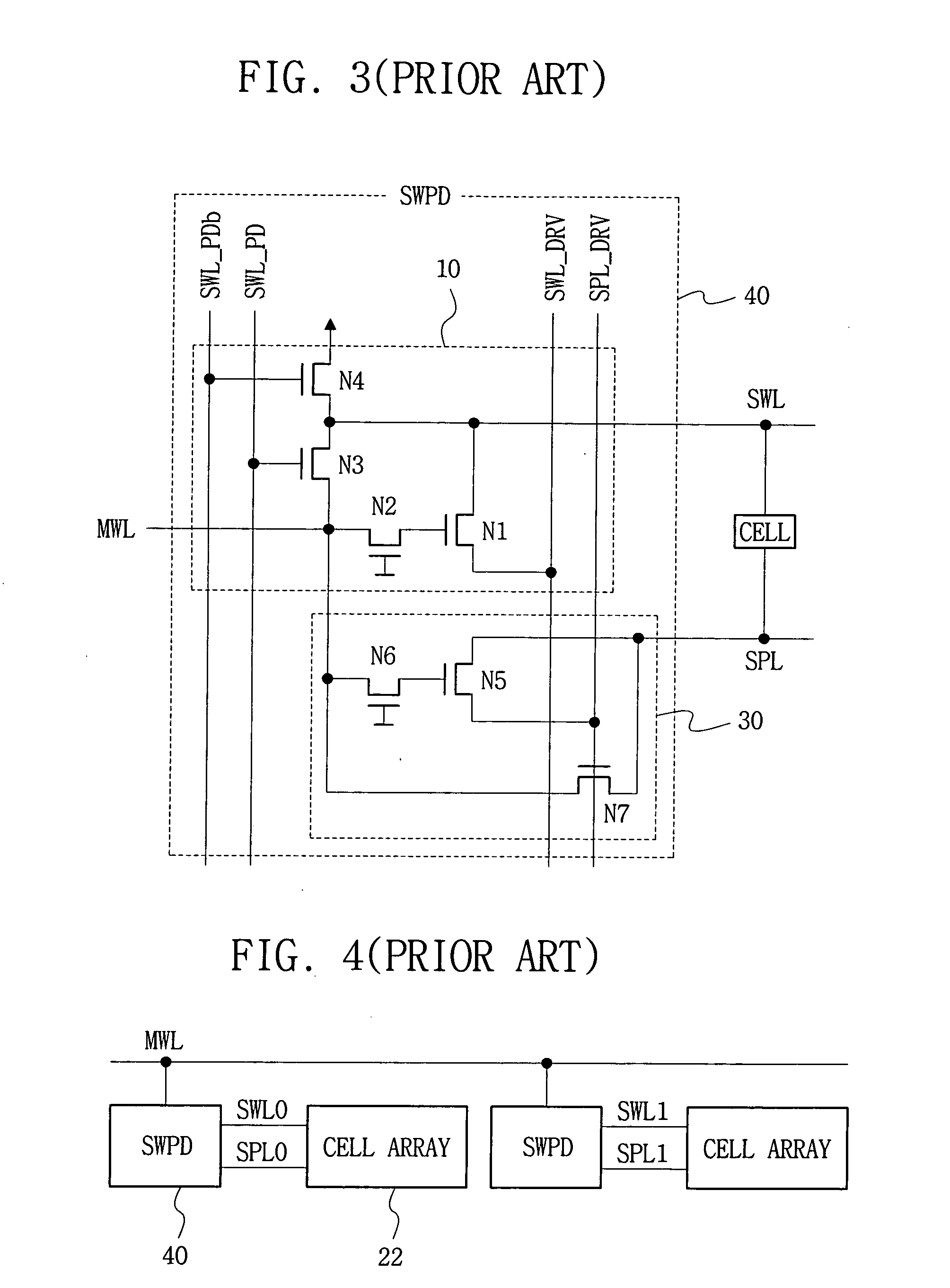
[0044] Referring to FIG. 5, a word line driver circuit in a semiconductor memory device according to an exemplary embodiment has a three-stage structure: of a main word line MWL controlled by a word line decoder circuit (not shown); sub word lines SWL controlled by sub word line driver circuits; and local word lines LWL controlled by local word line driver circuits LWD.

[0045] For example, in FIG. 5 there is shown o...


PUM


Abstract

A semiconductor memory device having a word line driver circuit configured in stages. A plurality of sub word line driver circuits are connected, in parallel, to each main word line, and provide a sub word line enable signal to a selected sub word line in response to a main word line enable signal provided through a main word line. A plurality of (local) word line driver circuits are connected in parallel, to each sub word line and provide a local word line enable signal to a selected local word line in response to the (main/sub) word line enable signal so as to operate a plurality of memory cells connected to the selected local word line. The transistor count and layout area of a semiconductor memory device decreases and a reduced chip area can be achieved.

Description

BACKGROUND OF THE INVENTION [0001] 1. Field of the Invention [0002] The present invention relates to a semiconductor memory device having a word line driver circuit, and more particularly to a word line driver circuit and a plate line driver circuit having stages and a reduced chip area. [0003] 2. Description of the Related Art [0004] A semiconductor memory device operating at a low voltage generally employs a voltage boosting circuit to apply a voltage higher than the nominal supply voltage so as to increase the operating speed and the reliability of reading or writing data in a memory cell. In this manner, a voltage corresponding to data applied to a bit line is transferred to a capacitor of a memory cell without a drop of threshold voltage in an access transistor of a memory cell, or data (charge) stored in the capacitor is passed to the bit line without a drop of threshold voltage of the access transistor, to prevent or substantially reduce errors in read or write operations. [0...

Claims


Application Information

Patent Timeline
Patent Type & Authority Applications(United States)
IPC IPC(8): G11C8/00
CPCG11C8/08G11C8/14G11C8/18G11C11/221G11C11/2257
Inventor JEON, BYUNG-GILMIN, BYUNG-JUNLEE, KANG-WOONLEE, HAN-JOO
Owner SAMSUNG ELECTRONICS CO LTD
Why Eureka
Try Eureka