Semiconductor memory device and a method for arranging signal lines thereof
a memory device and semiconductor technology, applied in the field of semiconductor memory devices, can solve problems such as the increase in the number of abnormal operations
- Summary
- Abstract
- Description
- Claims
- Application Information
AI Technical Summary
Benefits of technology
Problems solved by technology
Method used
Image
Examples
first embodiment
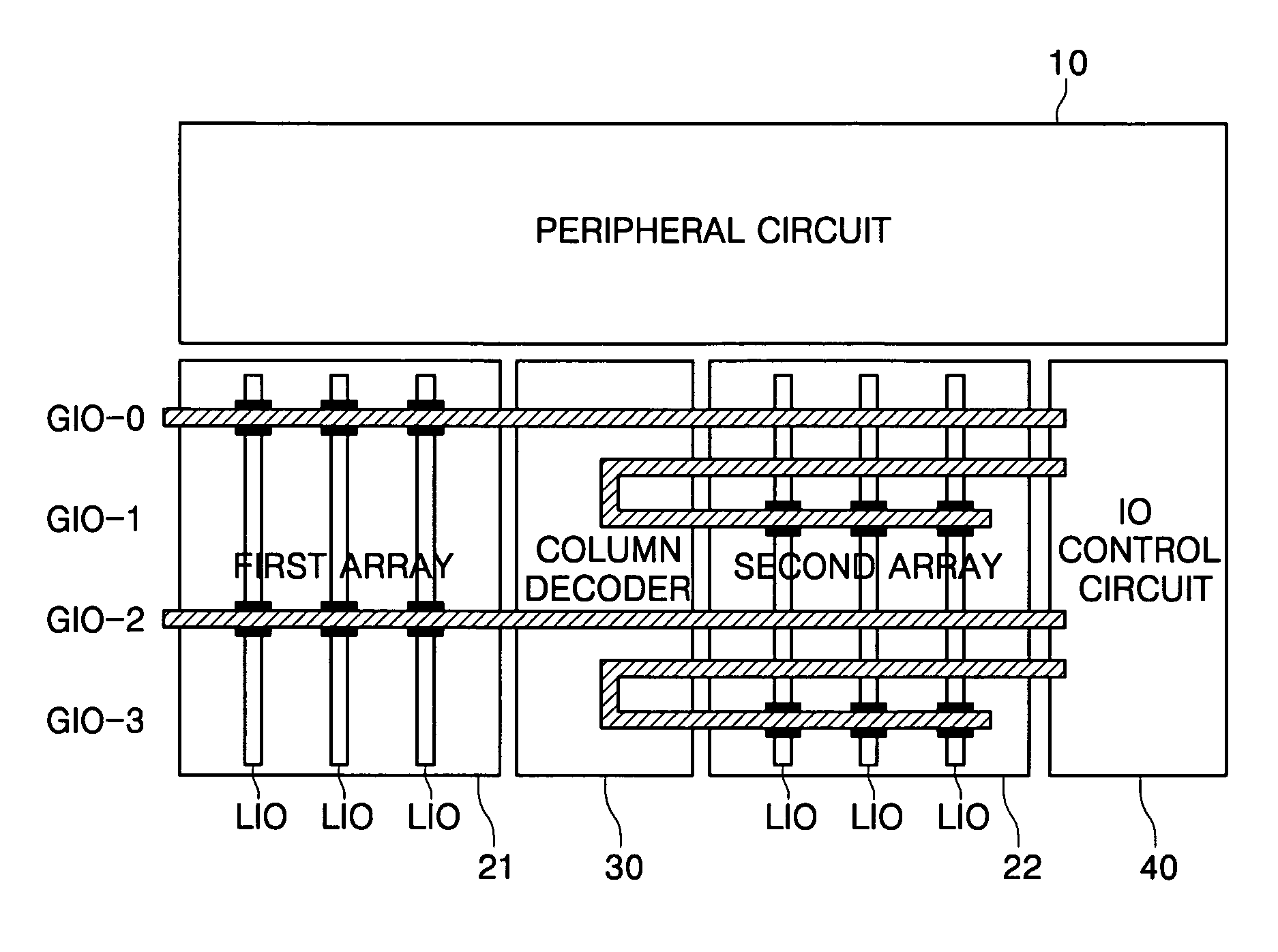
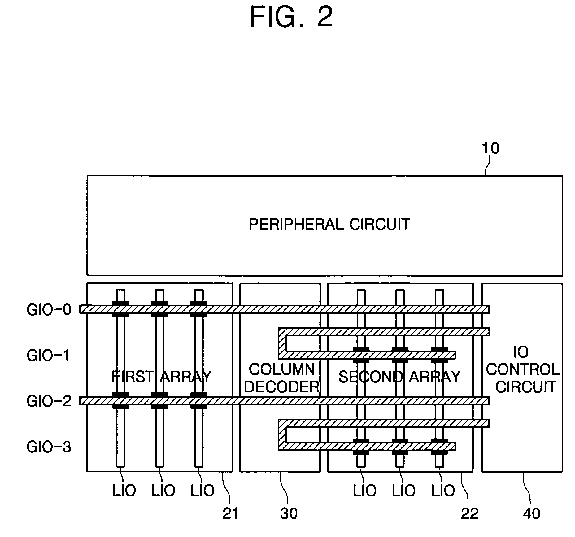
[0044]FIG. 2 is a schematic view illustrating a signal line arrangement of a semiconductor memory device according to the present invention.
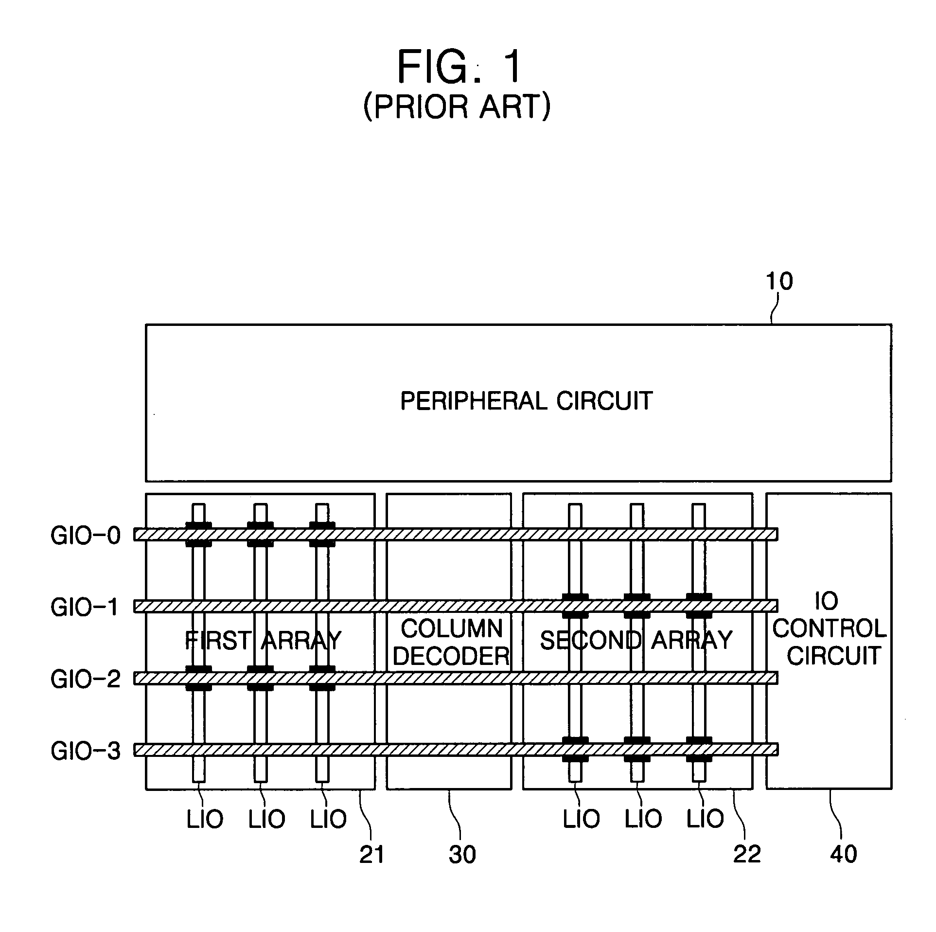
[0045] The function and arrangement of a peripheral circuit 10, first and second memory cell arrays 21 and 22, and IO control circuit 40 of FIG. 2 are the same or similar to those described above with reference to FIG. 1. In addition, the local data IO signal lines LIO of FIG. 2 are arranged in the same or similar fashion as shown in FIG. 1. As in FIG. 1, non-hatched signal lines are arranged on the first layer and hatched signal lines are arranged on the second layer. Global data IO signal lines GIO-0 and GIO-2, which are connected to the local data IO signal lines LIO above the first memory cell array 21 region, are also arranged in the same or similar way as shown in FIG. 1.
[0046] As shown in FIG. 2, global data IO signal lines GIO-1 and GIO-3, which are connected to the local data IO signal lines LIO above the second memory cell array 22 re...
second embodiment
[0048]FIG. 3 is a schematic view illustrating a signal line arrangement of a semiconductor memory device according to the present invention. The function and arrangement of a peripheral circuit 10, first and second memory cell arrays 21 and 22, and IO control circuit 40 of FIG. 3 are the same or similar to those described above with reference to FIG. 1. In addition, the local data IO signal lines LIO of FIG. 3 are arranged in the same or similar fashion as shown in FIG. 1. As in FIG. 1, non-hatched signal lines are arranged on the first layer and hatched signal lines are arranged on the second layer.
[0049] As shown in FIG. 3, a global data IO signal line GIO-1 of global data signal lines GIO-1 to GIO-3 which are connected to the local data IO signal lines LIO above the second memory cell array 22 region extends from the IO control circuit 40, passes over the peripheral circuit 10, takes a U-like turn above the column decoder 30 region and extends to the second memory cell array 22 r...
third embodiment
[0051]FIG. 4 is a schematic view illustrating a signal line arrangement of a semiconductor memory device according to the present invention. The function and arrangement of a peripheral circuit 10, first and second memory cell arrays 21 and 22, and 10 control circuit 40 of FIG. 4 are the same or similar to those described above with reference to FIG. 1. In addition, the local data IO signal lines LIO of FIG. 4 are arranged in the same or similar fashion as shown in FIG. 1. As in FIG. 1, non-hatched signal lines are arranged on the first layer and hatched signal lines are arranged on the second layer. Signal lines filled with dots in FIG. 4 are arranged on a third layer.
[0052] As shown in FIG. 4, global data IO signal lines GIO-1 and GIO-3 which are connected to the local data IO signal lines LIO above the second memory cell array 22 region are arranged such that portions which extend from the IO control circuit 40 to the column decoder 30 region without being connected to the local ...
PUM
 Abstract
Description
Claims
Application Information
 - R&D
- Intellectual Property
- Life Sciences
- Materials
- Tech Scout
- Unparalleled Data Quality
- Higher Quality Content
- 60% Fewer Hallucinations
Browse by: Latest US Patents, China's latest patents, Technical Efficacy Thesaurus, Application Domain, Technology Topic, Popular Technical Reports.
© 2025 PatSnap. All rights reserved.Legal|Privacy policy|Modern Slavery Act Transparency Statement|Sitemap|About US| Contact US: help@patsnap.com


