Optical delay element
a delay element and optical technology, applied in the field of optical delay elements, can solve the problems of large size of optical devices, difficult to compact optical devices, and large volume of optical devices, and achieve the effect of reducing the volume of line defects and enlarge the wavelength region
- Summary
- Abstract
- Description
- Claims
- Application Information
AI Technical Summary
Benefits of technology
Problems solved by technology
Method used
Image
Examples
first embodiment
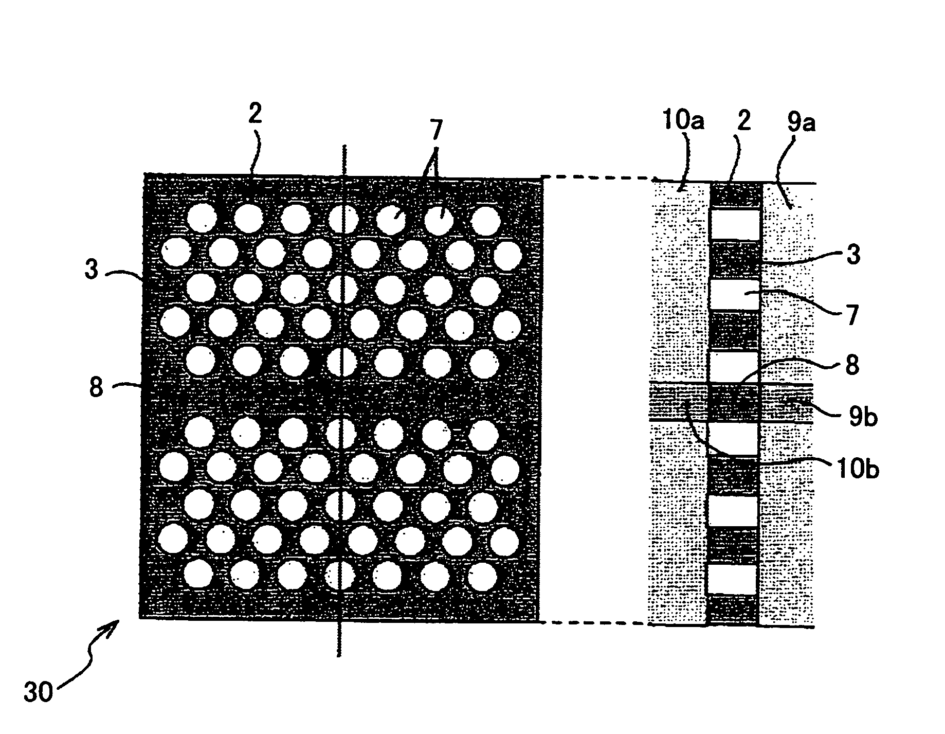
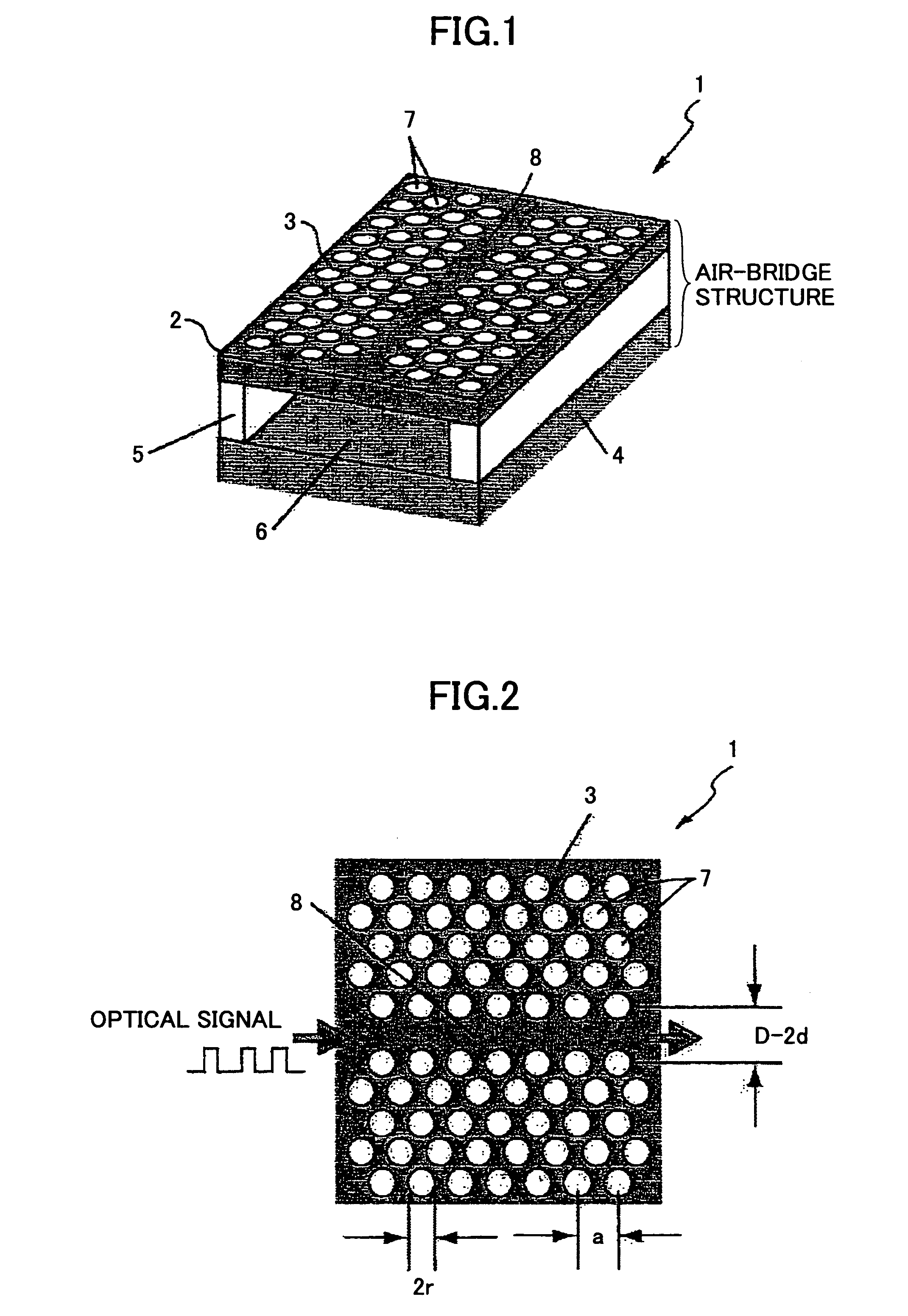
[0080]FIG. 1 is a perspective view for schematically illustrating an optical delay element 1 according to a first embodiment of the present invention, which includes a line defect optical waveguide formed from a two-dimensional photonic crystal slab.
[0081]FIG. 2 is a plan view of the optical delay element 1 in FIG. 1.
[0082] As illustrated in FIG. 1, the optical delay element 1 includes a substrate 4, pedestals 5 standing on the substrate 4, a high refractive index thin film 2 arranged on the pedestals 5, a cladding portion 6, which is actually an air space, and a photonic crystal structure 3 formed in the high refractive index thin film 2. For example, the thickness of the high refractive index thin film 2 is less than 1 μm. The photonic crystal structure 3 includes holes 7 filled with air. Because the cladding portion 6 is an air space, the structure of the optical delay element 1 is called an “air-bridge structure”.
[0083] If the refractive index of the high refractive index thi...
second embodiment
[0171] Expansion of a frequency region resulting in a large group refractive index, as described in the first embodiment, occurs even in a photonic crystal including a slab of a different refractive index.
[0172] In this embodiment, descriptions are made of an optical delay element in which the equivalent refractive index of the high refractive index thin film 2 is about two. In the present embodiment, the same reference numbers are assigned to the same elements as described in the previous embodiment, and overlapping descriptions are omitted.
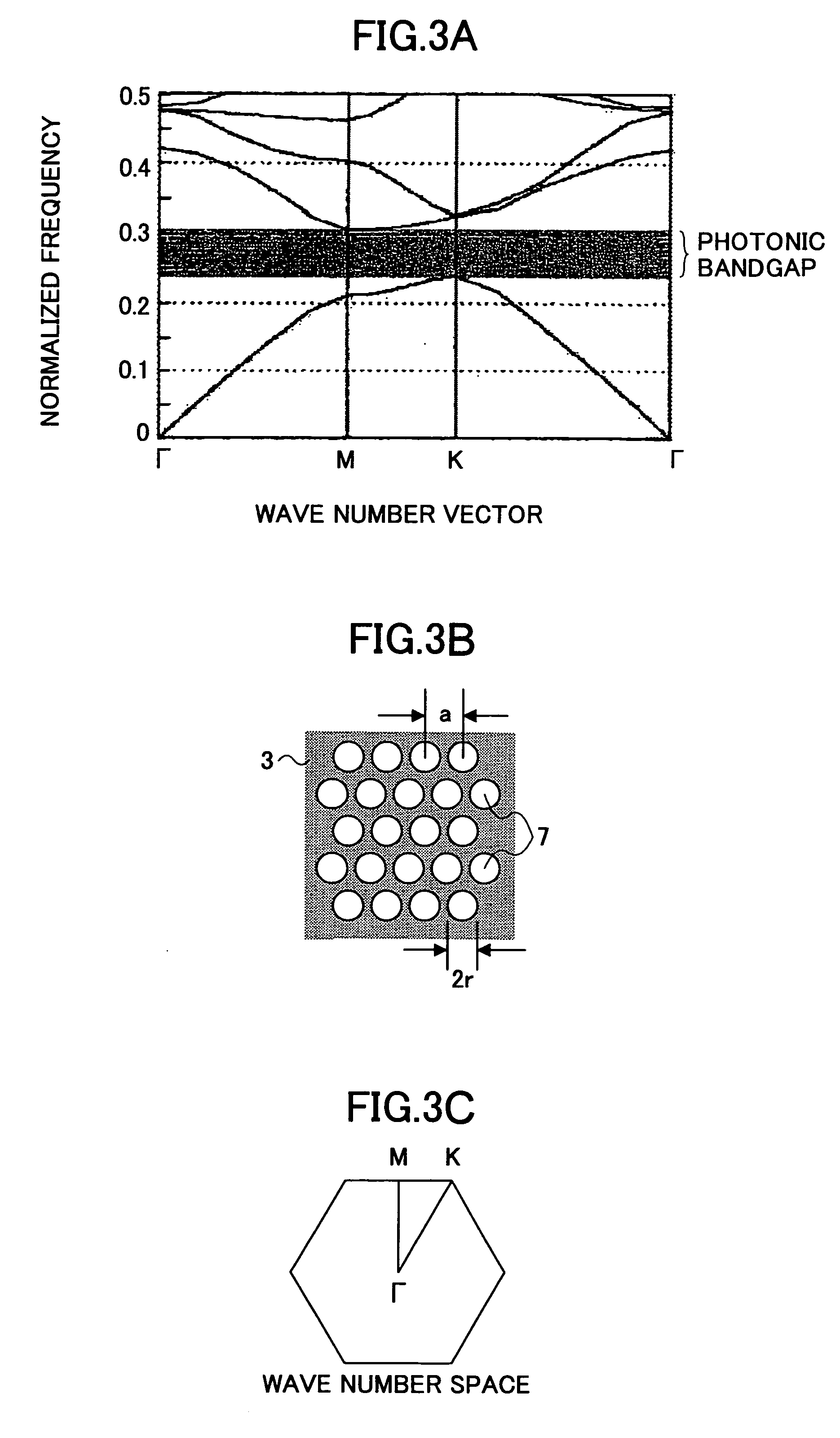
[0173] In a photonic crystal, if the contrast of refractive index is approximately two, a photonic bandgap appears in the photonic crystal. However, in the case of the two-dimensional photonic crystal slab structure, because of strong influences of light lines, design tolerance becomes small.
[0174] For example, a thin film substrate 2 having an equivalent refractive index near two is made, and the photonic crystal structure 3 constituted from...
third embodiment
[0193] In this embodiment, a method is described of fabricating the optical delay element of the present invention. In the present embodiment, the same reference numbers are assigned to the same elements as described in the previous embodiment, and overlapping descriptions are omitted.
[0194] As described above, a two-dimensional photonic crystal can be fabricated with a SOI (silicon-on-insulator) substrate and semiconductor fine processing techniques.
[0195] With the latest SOI technology, a SOI substrate including a 0.2 μm-thick silicon layer is commercially available, and this SOI substrate can be used to fabricate the two-dimensional photonic crystal.
[0196] The triangular lattice of holes can be built by lithography and dry etching. For example, an electron-beam resist is applied on a substrate, then the resist is patterned by drawing circular holes having diameter of 400 nm in the resist with an electron beam. The diameter of the holes is decided by the object light wavelength...
PUM
 Abstract
Description
Claims
Application Information
 - R&D
- Intellectual Property
- Life Sciences
- Materials
- Tech Scout
- Unparalleled Data Quality
- Higher Quality Content
- 60% Fewer Hallucinations
Browse by: Latest US Patents, China's latest patents, Technical Efficacy Thesaurus, Application Domain, Technology Topic, Popular Technical Reports.
© 2025 PatSnap. All rights reserved.Legal|Privacy policy|Modern Slavery Act Transparency Statement|Sitemap|About US| Contact US: help@patsnap.com


