
Nonvolatile memory for logic circuits

Active Publication Date: 2006-04-20
KK TOSHIBA +1
View PDF5 Cites 60 Cited by
  • Summary
  • Abstract
  • Description
  • Claims
  • Application Information

AI Technical Summary

Benefits of technology

[0013] A memory circuit according to the present invention includes a volatile data storage circuit and at least one nonvolatile memory coupled within the volatile data storage circuit, wherein the at least one nonvolatile memory includes a high resistive state and a low resistive state. The volatile data storage circuit can include, for example, cross-coupled inverters, cross-coupled NAND gates, or another volatile data storage circuit. The nonvolatile memories can include, for example, a spin-injection magnetic tun

Problems solved by technology

Currently, logic circuits and processors based on these sequential circuits consume high amounts of power.
Further, it is expected that the power consumption will increase with decreasing dimensions of semiconductor components utilized in the sequential logic circuit.
In particular, in the generation after the current MOSFET 65 nm technology, it is expected that static power consumption due to gate electrode leakage will become larger than the dynamic power consumption due to turning on and off of MOSFET transistors.
However, the reduction of supply voltage should be limited in these methods because data stored in volatile memory cells may be easily lost when supply voltages are reduced.
Further, static gate leakage, which increases as the gate oxide becomes thinner, is inevitable.
Therefore, the real effects of these types of power consumption reducing techniques are limited.
This technique is not possible in conventional sequential logic circuits because, as soon as the power is shut off, the data stored in the circuit is lost.
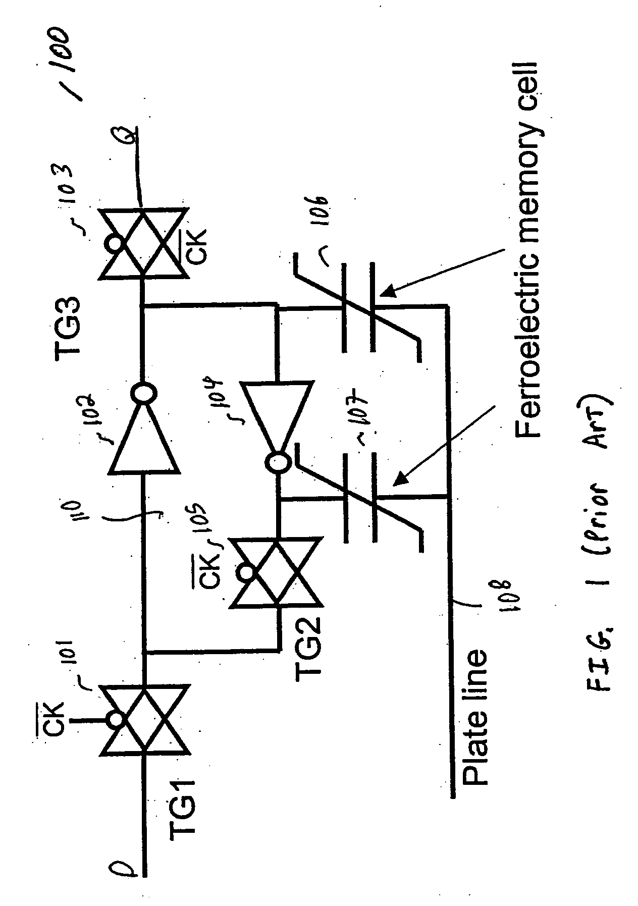
Many ferroelectric materials used in Ferroelectric memory cells, however, exhibit poor endurance when subjected to repeated write / erase operations.
In many cases, the endurance is limited to about 1014 operations even for high quality ferroelectric materials formed directly on a silicon substrate.
The endurance may be seriously degraded for ferroelectric materials stacked on silicon devices on a silicon substrate.
Because memories in logic circuits are repeatedly rewritten in accordance with the clock signal, a typical number of operations exceeds 1014 in a single month of operation in a 100 MHz clock, after which the logic circuits may become unreliable or no longer function.
In addition to the endurance difficulties, high quality ferroelectric materials are only formed directly on a silicon substrate and cannot easily be stacked.

Method used


Image

  • Nonvolatile memory for logic circuits
  • Nonvolatile memory for logic circuits
  • Nonvolatile memory for logic circuits

Examples


Embodiment Construction

[0042]FIG. 2 illustrates a combination of sequential logic circuits that can utilize memory circuits according to some embodiments of the present invention. As shown in FIG. 2, a sequential logic circuit 201 stores data for a combinational logic circuit 202. Further, once the operations of combinational logic circuit 202 are completed, the result can be stored in a sequential logic circuit 201. Each of sequential logic circuits 201 is clocked with a clock signal 203. One skilled in the art will recognize that a combinational logic circuit 202 can receive data stored in more than one sequential logic circuit 201. In embodiments of the present invention, sequential logic circuits 201 include non-volatile memory cells that retain data when power is shut down to the sequential logic circuit.

[0043]FIG. 3 illustrates a memory layout with memory arrays 302 and 303 according to embodiments of the present invention. Each of memories 302 and 303 include non-volatile memory cells. As is shown...


PUM


Abstract

A memory circuit that retains stored data upon power down includes a volatile data storage circuit; and at least one nonvolatile memory coupled within the volatile data storage circuit, wherein the at least one nonvolatile memory includes a high resistive state and a low resistive state. The volatile data storage circuit can include cross-coupled inverters, cross- coupled NAND gates, or another volatile data storage circuit. The nonvolatile memories can include a spin-injection magnetic tunnel junction memory, a magnetic tunnel junction memory, a metal insulator phase change memory, an organic memory, or some other memory with two resistive states.

Description

RELATED APPLICATIONS [0001] The present application claims priority to Provisional Application No. 60 / 620,236, “Nonvolatile Sequential Circuits,” by Shinobu Fujita and Thomas H. Lee, filed on Oct. 18, 2004, which is herein incorporated by reference in its entirety.BACKGROUND [0002] 1. Field of the Invention [0003] The present invention relates to memory circuits and, in particular, to memory circuits with nonvolatile memories. [0004] 2. Discussion of Related Art [0005] Sequential logic circuits are utilized in numerous systems. Currently, logic circuits and processors based on these sequential circuits consume high amounts of power. Further, it is expected that the power consumption will increase with decreasing dimensions of semiconductor components utilized in the sequential logic circuit. In particular, in the generation after the current MOSFET 65 nm technology, it is expected that static power consumption due to gate electrode leakage will become larger than the dynamic power c...

Claims


Application Information

Patent Timeline
IPC IPC(8): G11C11/22
CPCG11C5/02G11C11/005G11C14/0081
Inventor FUJITA, SHINOBULEE, THOMAS H.
Owner KK TOSHIBA
Learn More