
Transistor with high dielectric constant gate and method for forming the same

a transistor gate, high dielectric constant technology, applied in the direction of semiconductor devices, basic electric elements, electrical appliances, etc., can solve the problems of inability to tolerate the thinnest gate dielectric of 0.8 nanometers, inability to remove such materials from the non-gate region where they are not needed, and even for high-performance systems

Inactive Publication Date: 2006-03-23
TAIWAN SEMICON MFG CO LTD
View PDF5 Cites 40 Cited by
  • Summary
  • Abstract
  • Description
  • Claims
  • Application Information

AI Technical Summary

Benefits of technology

[0006] To address the above needs and in view of its purposes, an aspect of the invention provides a method for forming a semiconductor device. The method comprises forming a high-k gate dielectric material over a substrate including over a gate region, using a planarization step such as chemical mechanical polishing to remove the high-k gate dielectric material from regions other than the gate region, and forming a conductive materi...

Problems solved by technology

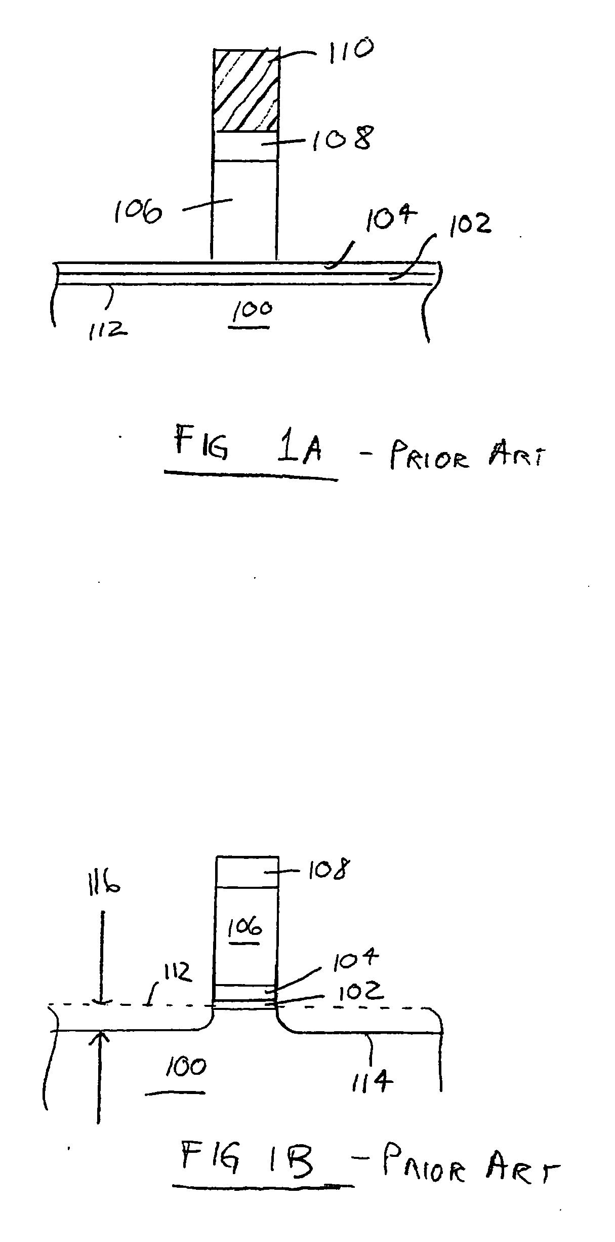
It is considered that tunneling currents arising from silicon dioxide (SiO2) gate dielectrics thinner than 0.8 nanometers cannot be tolerated, even for high-performance systems.
Replacing the conventional SiO2 gate material with a high-dielectric constant (high-k) dielectric gate material, however, presents other challenges.
One challenge associated with the use of high-k gate dielectric material is the inability to sufficiently remove such materials from the non-gate regions where they are not needed.

Method used


Image

  • Transistor with high dielectric constant gate and method for forming the same
  • Transistor with high dielectric constant gate and method for forming the same
  • Transistor with high dielectric constant gate and method for forming the same

Examples


Embodiment Construction

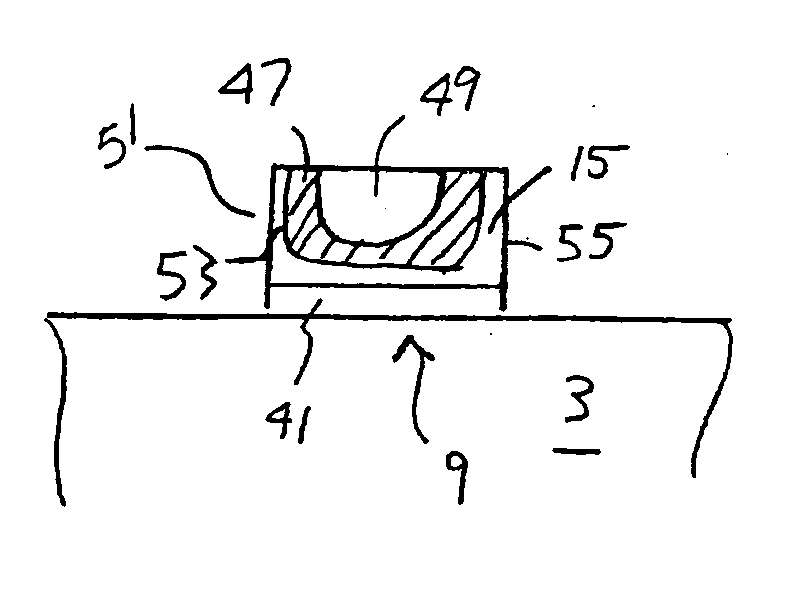
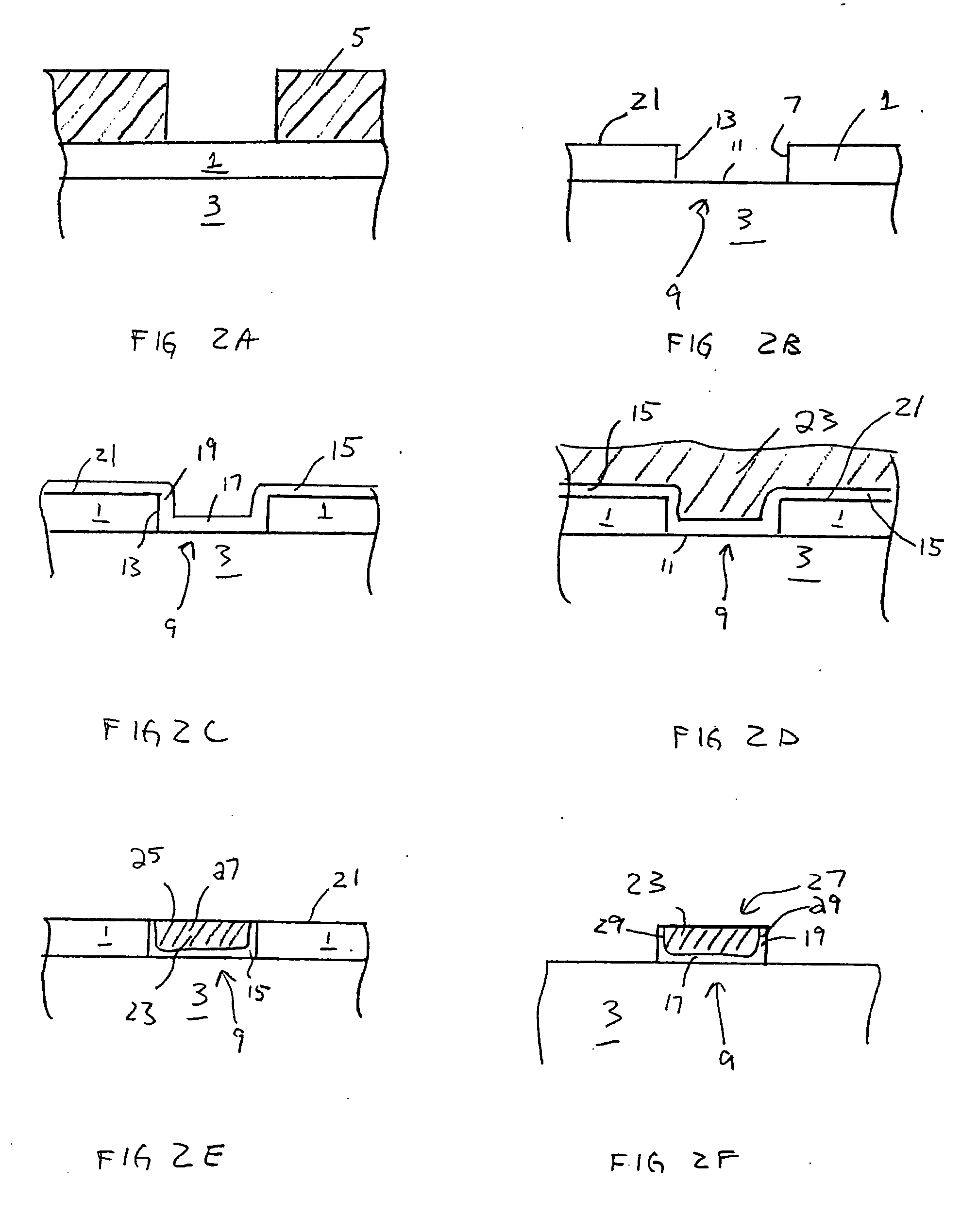
[0013]FIG. 2A shows a layer of organic material 1 formed over substrate 3. Patterned photoresist 5 is formed above organic material 1. Photoresist 5 pattern enables the formation of an opening in organic material 1 over gate region 9. Organic material 1 may be an organic low dielectric constant spin-on-polymer (SOP) material such as a fluorinated poly (arylene ether) organic polymer commercially available as FLARE from Allied Signal Corporation, 1349 Moffett Park Drive, Sunnyvale, Calif. 94089, or PAE-2 produced by Schumacher Corporation, 1969 Palomar Oaks Way, Carlsbad, Calif. 92009. A further commercial fluorinated organic poly(arylene ether) low dielectric constant spin-on-polymer (SOP) dielectric material that may be used as organic material 1 is SILK, available from Dow Chemical Co., 1712 Building, Midland, Mich. 48674. In another embodiment, APF, by Applied Materials Inc, may be used as organic material 1. Other suitable materials may be used as organic material 1, in other ex...


PUM


Abstract

A semiconductor device provides a gate structure that includes a conductive portion and a high-k dielectric material formed beneath and along sides of the conductive material. An additional gate dielectric material such as a gate oxide may be used in addition to the high-k dielectric material. The method for forming the structure includes forming an opening in an organic material, forming the high-k dielectric material and a conductive material within the opening and over the organic material then using chemical mechanical polishing to remove the high-k dielectric material and conductive material from regions outside the gate region.

Description

FIELD OF THE INVENTION [0001] The present invention relates, most generally to a semiconductor device and methods for forming the same. More particularly, the invention relates to a high dielectric constant transistor gate and a method for forming such a structure. BACKGROUND [0002] Shrinking the conventional MOSFET (metal oxide semiconductor field effect transistor) beyond the 50 nanometer technology node requires innovations to circumvent barriers due to the fundamental physics that constrain conventional MOSFETs. Continued device shrinkage requires a reduction of gate dielectric thickness. This requirement arises from two different considerations: controlling the short-channel effect, and achieving a high current drive by keeping the amount of charge induced in the channel as large as possible as the power-supply voltage decreases. It is the reduction of the equivalent electrical thickness of the gate dielectric that is important in achieving each of the aforementioned considerat...

Claims


Application Information

Patent Timeline
IPC IPC(8): H01L21/8238H01L21/302
CPCH01L21/28079H01L21/28088H01L29/495H01L29/66583H01L29/517H01L29/518H01L29/66553H01L29/4975
Inventor HSU, JU-WANGSHIEH, JYU-HORNGCHIANG, JU-CHIEN
Owner TAIWAN SEMICON MFG CO LTD
Learn More