Switching control circuit having off-time modulation to improve efficiency of primary-side controlled power supply
- Summary
- Abstract
- Description
- Claims
- Application Information
AI Technical Summary
Benefits of technology
Problems solved by technology
Method used
Image
Examples
Embodiment Construction
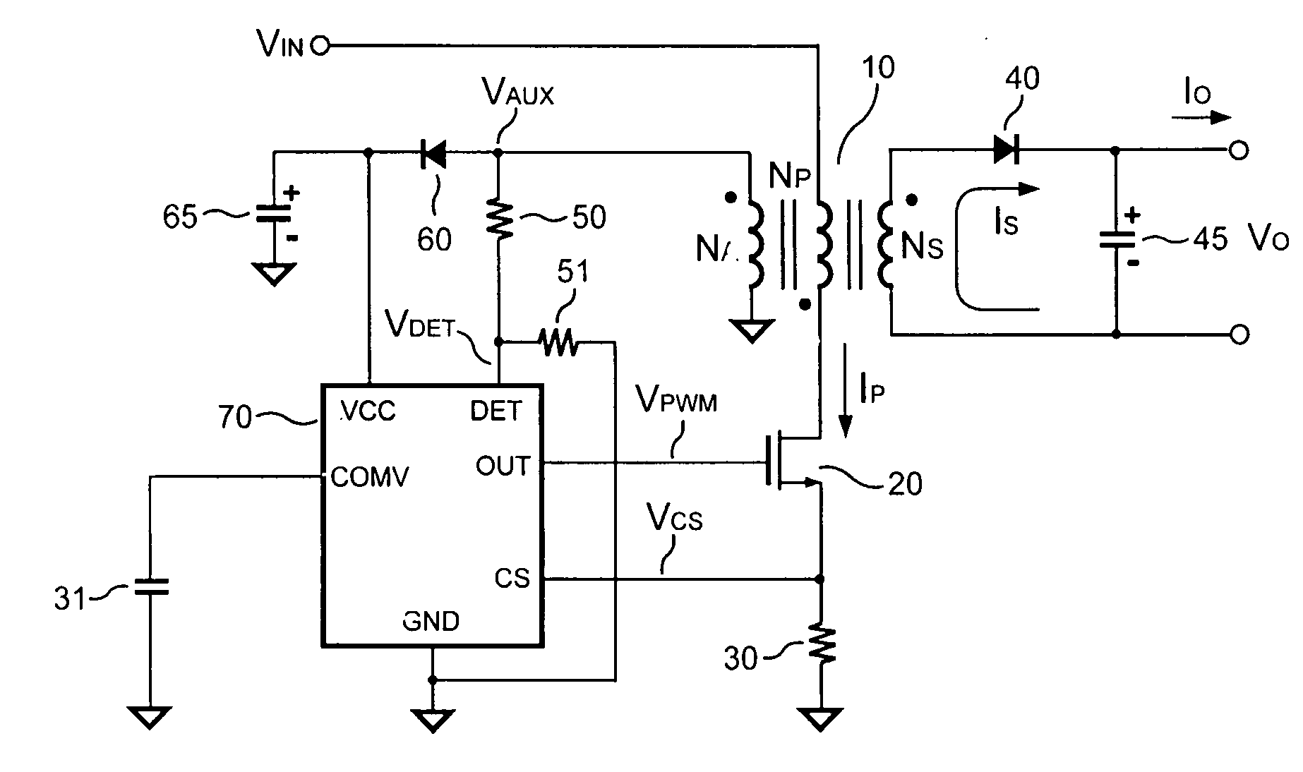
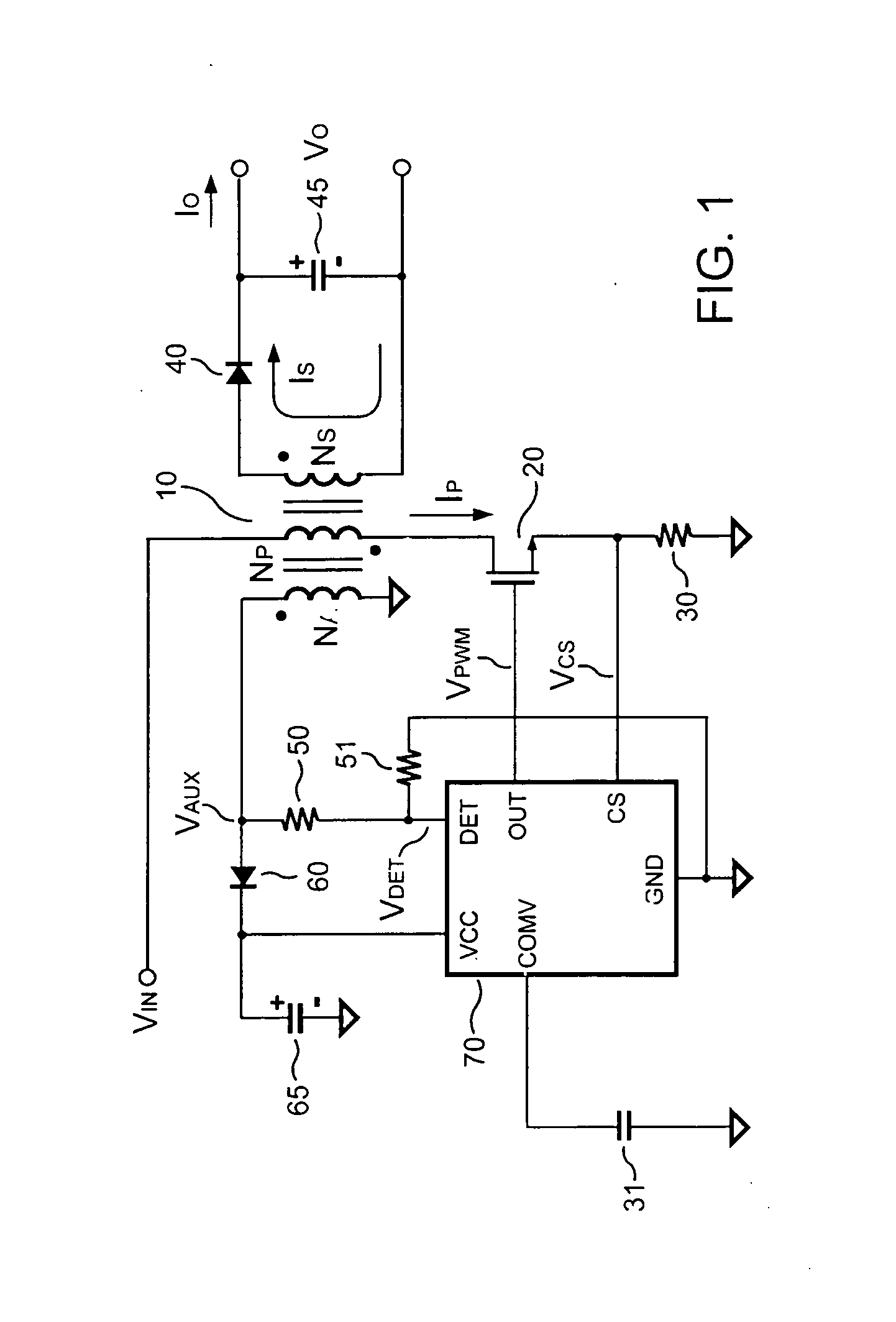
[0017]FIG. 1 shows a power supply. The power supply includes a transformer 10 comprising an auxiliary winding NA, a primary winding NP, and a secondary winding NS. The primary winding NP is coupled to an input voltage VIN of the power supply. In order to regulate an output voltage VO and / or an output current IO of the power supply, a switching control circuit includes a switching signal VPWM to control a switch, such as a transistor 20. A controller 70 generates the switching signal VPWM.
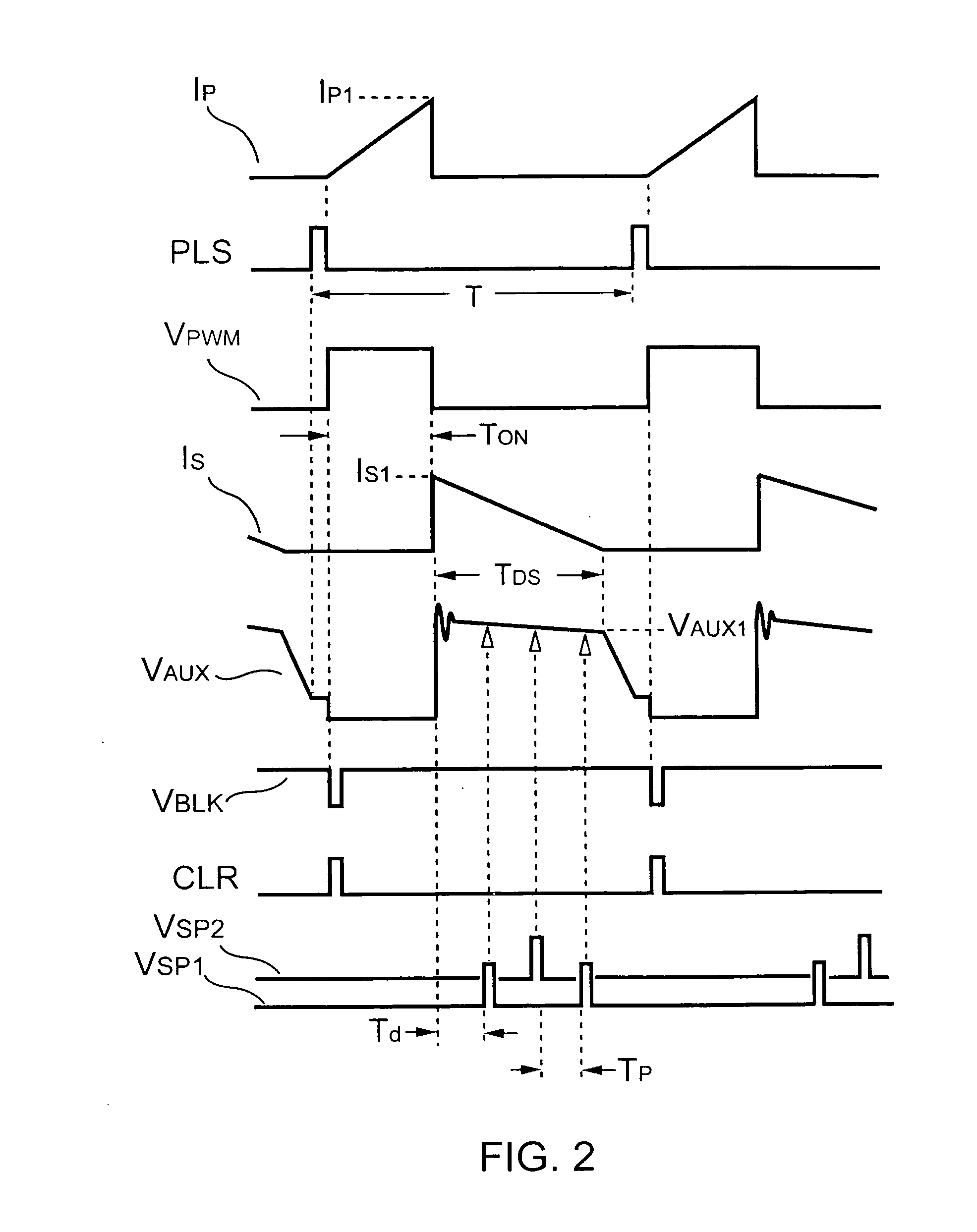
[0018]FIG. 2 shows various signal waveforms of the power supply in FIG. 1. As the switching signal VPWM is logic-high, a primary-side switching current IP will be generated accordingly. A primary-side switching peak current IP1 can be given by, IP1=VINLP×TON(1)
[0019] where LP is the inductance of the primary winding NP of the transformer 10; TON is an on-time of the switching signal VPWM.
[0020] Once the switching signal VPWM is logic-low, the energy stored in the transformer 10 will be transferre...
PUM
 Abstract
Description
Claims
Application Information
 - R&D
- Intellectual Property
- Life Sciences
- Materials
- Tech Scout
- Unparalleled Data Quality
- Higher Quality Content
- 60% Fewer Hallucinations
Browse by: Latest US Patents, China's latest patents, Technical Efficacy Thesaurus, Application Domain, Technology Topic, Popular Technical Reports.
© 2025 PatSnap. All rights reserved.Legal|Privacy policy|Modern Slavery Act Transparency Statement|Sitemap|About US| Contact US: help@patsnap.com


