Planar lightwave circuit package

a lightwave circuit and circuit technology, applied in the field of optical telecommunications packaging arrangement, can solve the problems of adversely affecting the performance of the photodetector, and achieve the effect of a relatively cost-effective solution

Inactive Publication Date: 2006-02-16
LUMENTUM OPERATIONS LLC
View PDF8 Cites 5 Cited by
  • Summary
  • Abstract
  • Description
  • Claims
  • Application Information

AI Technical Summary

Benefits of technology

[0018] It is a feature of the invention that the faceplate and a photodetector carrier can form a hermetic cavity while allowing optical energy to reach the photodetector array through the transparent cores of the faceplate. The faceplate thus offers a sealing function in an economical manner (without necessitating a hermetic enclosure over the entire PLC circuit) while also providing transparency for collimated light transmission from the PLC, either through free-space or direct coupling.

Problems solved by technology

It is important to keep the photodetector(s) in a hermetically sealed housing as contaminants such as dust particles, water vapor or condensate, dust, fumes, smoke and other pollutants can adversely affect the photodetector's performance.
This however is a relatively costly solution.

Method used


Image

  • Planar lightwave circuit package
  • Planar lightwave circuit package
  • Planar lightwave circuit package

Examples


Embodiment Construction

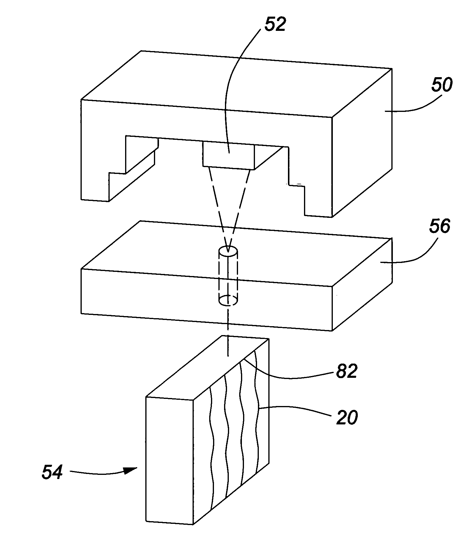
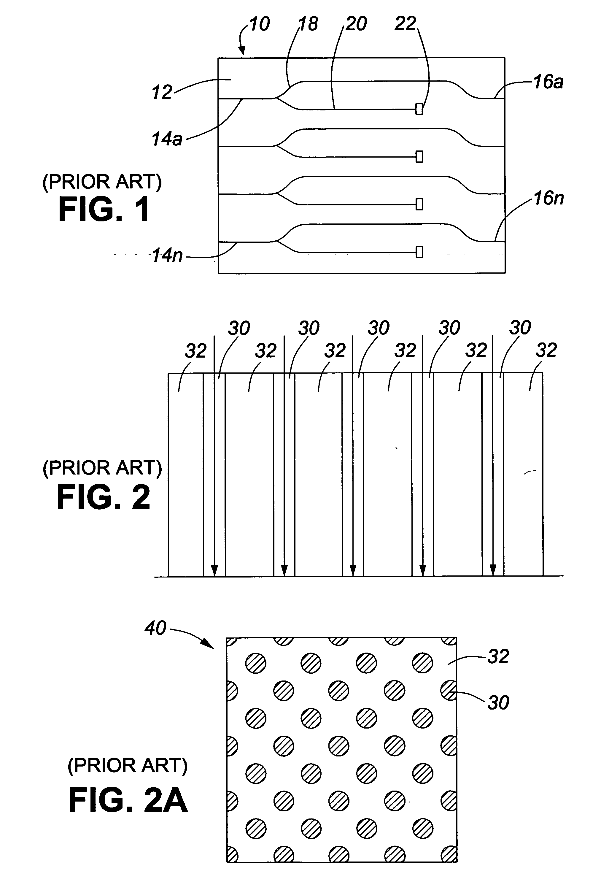
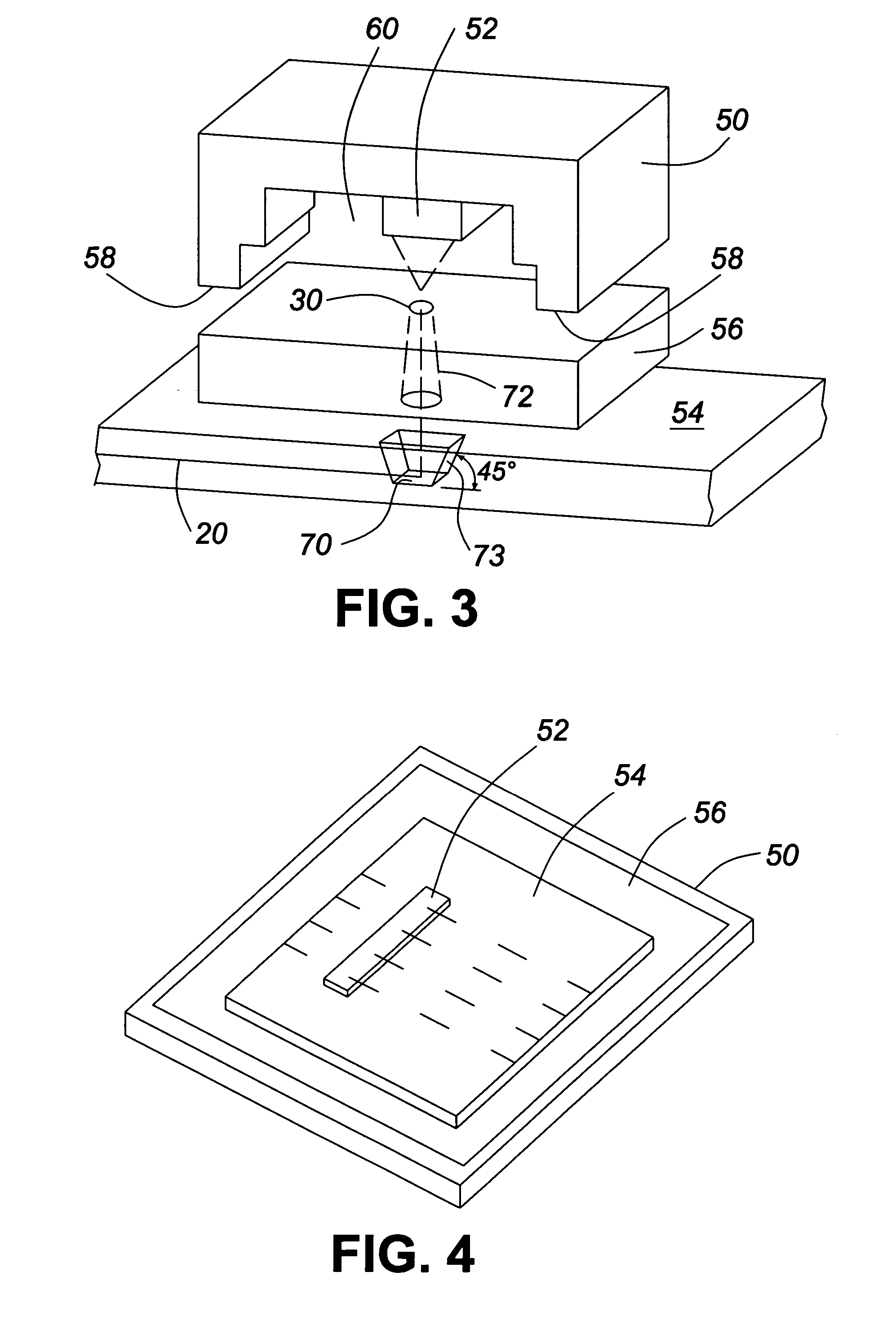
[0027] Turning first to FIG. 1 (prior art), a typical planar lightwave circuit (PLC) 10 is shown schematically. The PLC has a planar substrate 12, a plurality of input channel waveguides 14a-14n and a plurality of output channel waveguides 16a-16n. Each input waveguide is provided with a 5%-95% coupler 18 thus defining 95% arms extending into output waveguides 16a-16n, and a plurality of 5% arms 20. The 5% arm 20 of every coupler ends with a tap 22. The taps are formed by metallized mirror surfaces disposed at an angle, approximately 45°, to the propagation axis of a light beam propagating in the 5% arm 20.

[0028] The taps 22 can be made for example by etching the angled reflective surfaces into the waveguide followed by depositing gold onto the reflective surface using a sputtering process.

[0029] In an embodiment of the invention, the taps are created by RIE (reactive ion etching) of a 45-degree notch through the cladding and core, followed by deposition of a reflective metal coat...


PUM


Abstract

An optical packaging arrangement combines a planar lightwave circuit (PLC) having an array of waveguides thereon, an array of photodetectors on a substrate to receive light beams coupled out of the PLC by the output ports, and a collimating faceplate, having a plurality of glass cores, extending between the PLC and the photodetector array for coupling the output light beams to respective photodetectors. The faceplate forms a cover for a hermetic cavity encompassing the photodetectors. The PLC is disposed either co-planarly with the faceplate or transversely to it. Light from the PLC is tapped via a plurality of taps formed on the PLC for coupling to the photodetectors.

Description

RELATED APPLICATIONS [0001] None FIELD OF THE INVENTION [0002] This invention relates generally to optical data communication devices and more specifically, to a packaging arrangement for optical telecommunications, the arrangement including an array of optical input ports, e.g. a planar lightwave circuit, and a plurality of photodetectors, the optical input array being optically coupled with the photodectors. BACKGROUND OF THE INVENTION [0003] Planar lightwave circuits (PLC) are well known in optical communications. They are formed on various substrates and include a network of waveguides, for example channel waveguides. An example of a PLC is shown in U.S. Pat. No. 6,507,680 issued Jan. 14, 2003 to Nishimura et al. [0004] In the design of PLC architectures, it is important to properly integrate the taps and photodetectors with the optical transmission channels e.g. channel waveguides. In Nishimura, the photodetectors are integrated with the PLC and arranged for evanescent coupling...

Claims


Application Information

Patent Timeline
Patent Type & Authority Applications(United States)
IPC IPC(8): G02B6/12G02B6/122G02B6/34G02B6/42H01S5/022
CPCG02B6/12004G02B6/12019G02B6/4249G02B6/4214G02B6/4206
Inventor CRAFTS, DOUGLAS E.FARRELL, JAMES F.FARRELLY, MARK B.COOK, DUANEPEDDADA, SATYANARAYANA RAO
Owner LUMENTUM OPERATIONS LLC
Why Eureka
Try Eureka