Coupled cavity high power semiconductor laser

Inactive Publication Date: 2006-02-09
ARASOR ACQUISITION +1
View PDF17 Cites 108 Cited by
  • Summary
  • Abstract
  • Description
  • Claims
  • Application Information

AI Technical Summary

Benefits of technology

[0012] In accordance with certain method aspects of the present invention, the first active resonant cavity is epitaxially grown on the bottom surface of the substrate. The top surface of the substrate is provided with an anti-reflective coating and an external output mirror configured to control the desired mode or modes of the laser energy resonating both in the second passive resonant passive and in the first active cavity. In the preferred embodiment the external mirror is separated from the substrate and is configured to provide the desired fundamental mode output. In an alternative embodiment that takes particular advantage of the coupled-cavity configuration to reduce losses within the second passive cavity, the substrate may occupy the full extent of the second passive cavity and its top surface may be configured by binary optics techniques prior to depositing the required upper electrode and top reflector, to thereby produce monolithic fully integrated coupled cavity device.
[0013] Preferably, a non-linear frequency doubling material is included inside the second passive resonant cavity to thereby convert or reduce the output wavelength from the longer wavelengths associated with typical semiconductor laser materials, such as GaAs and GaInAs, to the shorter wavelengths necessary or desirable for various medical, materials processing, and display applications. In that case, the reflectivity characteristics of the various optical components are preferably chosen to favor the feedback of the unconverted fundamental wavelength back towards the active gain region and the output of any already converted harmonics through the output mirror.
[0014] As another option, a polarizing element which selectively favors a desired polarization orientation may be included within the second passive resonant cavity. Such a polarizing element may be in the form of a two-dimensional grid of conductive lines located at an anti-node of the optical energy resonating within the second passive resonant cavity to thereby absorb polarization parallel to those lines, and may be conveniently formed on the upper surface of the substrate adjacent to the anti-reflection layer.
[0018] An additional advantage of a coupled cavity device of certain exemplary embodiments of the present invention is that the output laser wavelength is determined by the Fabry-Perot resonance frequency of the active cavity and is tunable with temperature at the rate of about 0.07 nm per degree Centigrade for GalnAs type devices operating in the 980 nm wavelength region, thereby providing a convenient tuning mechanism for certain applications requiring a variable wavelength tunable output, in discrete jumps essentially corresponding to the possible resonances within the second passive cavity.
[0020] In a currently preferred embodiment, the non-linear optical material inside each passive cavity of the array converts an IR fundamental wavelength of each laser device to a corresponding visible harmonic wavelength, and the external output cavity mirror comprises a Volume Bragg grating (VBG) or other similar optical component that is substantially reflective at the fundamental frequency and substantially transmissive at the harmonic frequency. The efficiency of such a device can be further enhanced by the addition of a partially reflective coating at the fundamental wavelength on the VBG, to thereby establish a combined reflectivity of the VBG and the dielectric coating at the fundamental wavelength at substantially 100% in order to maximize the circulating fundamental laser power in the cavity for efficient non-linear conversion, while still avoiding unwanted laser oscillation outside the VBG bandwidth. The VBG used in an array of such devices may be either flat, which simplifies registration and alignment during manufacture, or may be configured to narrow the IR spectrum fed back into the active resonant cavity and to shape the spatial mode distribution inside the cavity, thereby reducing the size of the mode and compensating for any deformations in the semiconductor array.

Problems solved by technology

Conventional vertical cavity surface-emitting lasers (VCSELs) typically have two flat resonator cavity mirrors formed onto the two outer sides of a layered quantum-well gain structure, and are significantly limited in single spatial-mode output power, typically a few milliwatts.
While greater optical power can be achieved from conventional VCSEL devices by using larger emitting areas, such a large aperture device is not particularly practical for commercial manufacture or use, and produces an output which is typically distributed across many higher order spatial modes.
Since any heat produced in the active gain region must be removed through the relatively thick p-type substrate, the practical output power from such a device is limited to about 100 mW for pulsed operation and to only a few mW for continuous (“cw”) operation.
However, especially in an electrically pumped device with a relatively thick substrate inside the laser cavity, increasing the doping of the substrate (desirable to minimize carrier crowding and electrical resistance) also increases the optical loss at the laser wavelength and the overall efficiency of the device is correspondingly reduced.

Method used


Image

  • Coupled cavity high power semiconductor laser
  • Coupled cavity high power semiconductor laser
  • Coupled cavity high power semiconductor laser

Examples


Embodiment Construction

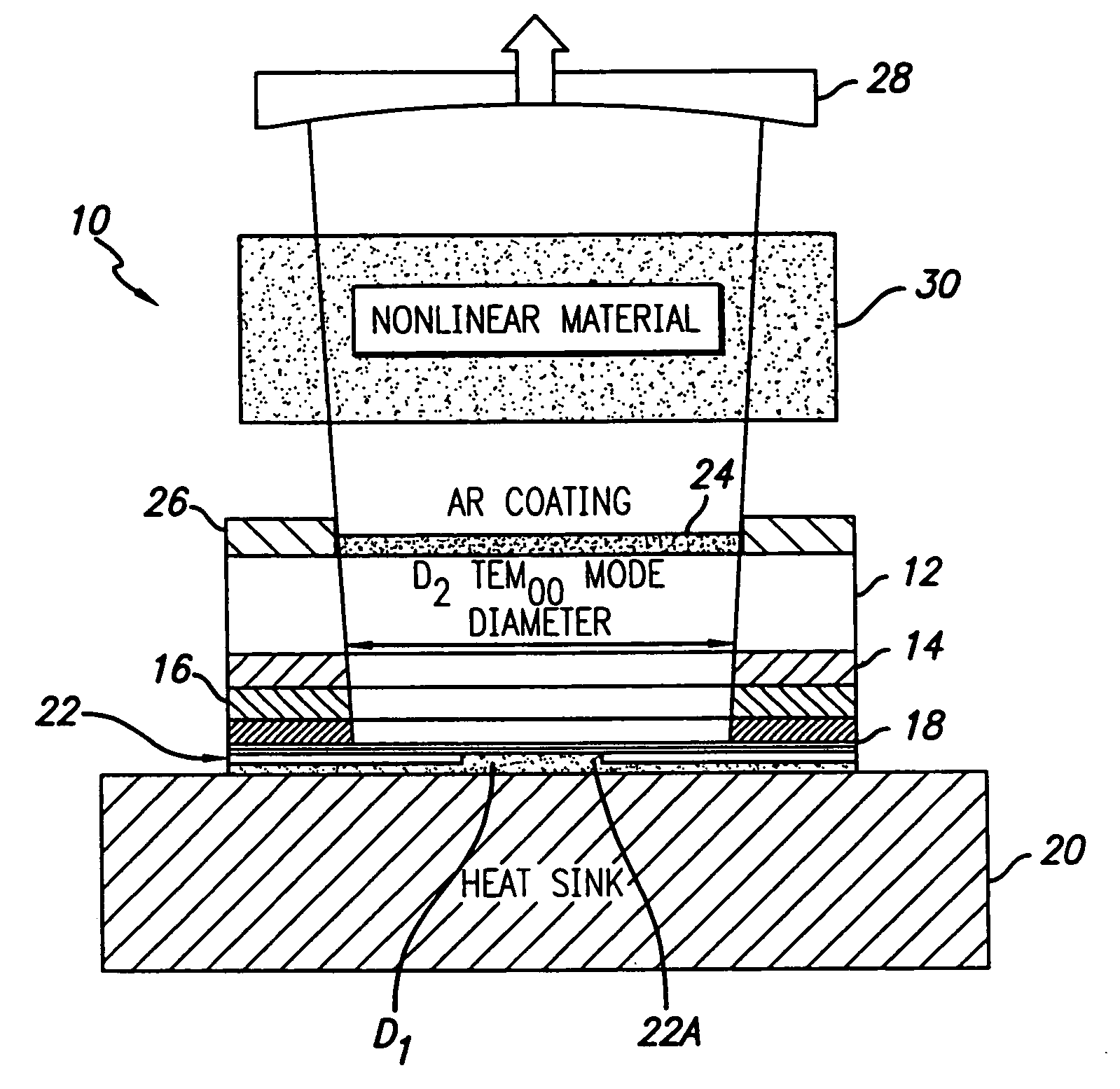
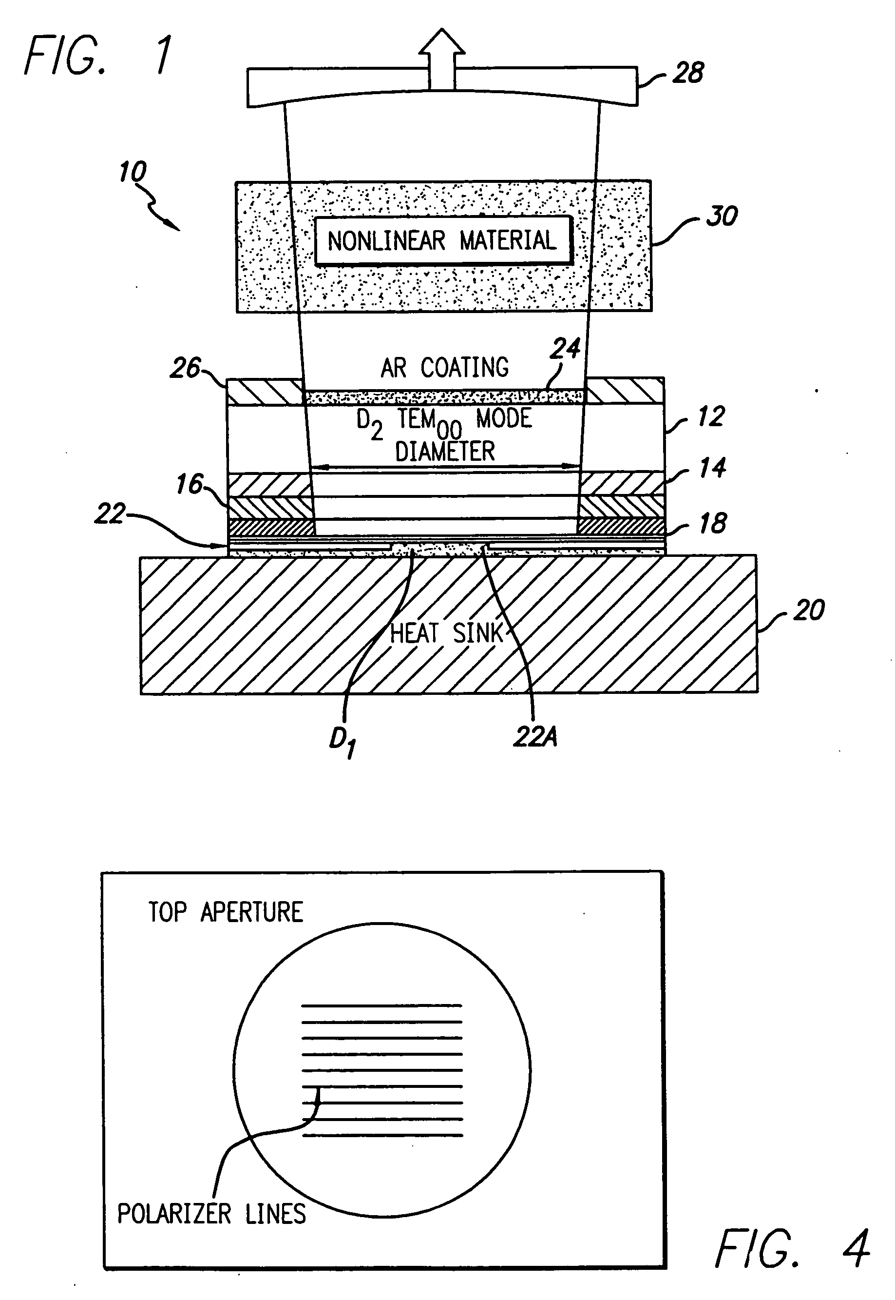
[0029] One preferred embodiment of a coupled cavity VECSEL 10 according to the present invention is shown schematically in FIG. 1. The coupled cavity VECSEL 10 includes an n-type semiconductor substrate 12. The substrate 12 should be sufficiently thick to be conveniently handled during manufacturing process and is sufficiently doped with n-type dopants to reduce the electrical resistance of substrate 12 to a value required for efficient operation and nearly uniform carrier injection across the current aperture region at high power levels (so that the active gain region is pumping uniformly without excessive carrier crowding), but without a corresponding sacrifice of the optical efficiency, as will be explained in detail in the following paragraphs. In an exemplary embodiment, the current aperture diameter is 100 μm and the doping level of the n-type dopants in the substrate is approximately between 1×10⁻¹⁷ cm−3 and 5×10⁻¹⁷ cm−3; the substrate is approximately 50 μm to 350 μm thick. ...


PUM


Abstract

An active gain region sandwiched between a 100% reflective bottom Bragg mirror and an intermediate partially reflecting Bragg mirror is formed on a lower surface of a supporting substrate, to thereby provide the first (“active”) resonator cavity of a high power coupled cavity surface emitting laser device. The reflectivity of the intermediate mirror is kept low enough so that laser oscillation within the active gain region will not occur. The substrate is entirely outside the active cavity but is contained within a second (“passive”) resonator cavity defined by the intermediate mirror and a partially reflecting output mirror, where it is subjected to only a fraction of the light intensity that is circulating in the gain region. In one embodiment, non-linear optical material inside each passive cavity of an array converts an IR fundamental wavelength of each laser device to a corresponding visible harmonic wavelength, and the external output cavity mirror comprises a Volume Bragg grating (VBG) or other similar optical component that is substantially reflective at the fundamental frequency and substantially transmissive at the harmonic frequency. The VBG used in an array of such devices may be either flat, which simplifies registration and alignment during manufacture, or may be configured to narrow the IR spectrum fed back into the active resonant cavity and to shape the spatial mode distribution inside the cavity, thereby reducing the size of the mode and compensating for any deformations in the semiconductor array.

Description

FIELD OF THE INVENTION [0001] This invention relates generally to surface-emitting semiconductor lasers. BACKGROUND OF THE INVENTION [0002] Conventional vertical cavity surface-emitting lasers (VCSELs) typically have two flat resonator cavity mirrors formed onto the two outer sides of a layered quantum-well gain structure, and are significantly limited in single spatial-mode output power, typically a few milliwatts. While greater optical power can be achieved from conventional VCSEL devices by using larger emitting areas, such a large aperture device is not particularly practical for commercial manufacture or use, and produces an output which is typically distributed across many higher order spatial modes. Several schemes have been proposed for increasing single-mode output power from surface-emitting devices. One approach is to replace one of the mirrors adjacent the active region of a conventional VCSEL device with a more distant reflector whose curvature and spacing from the acti...

Claims


Application Information

Patent Timeline
IPC IPC(8): H01S3/08H01S5/00
CPCH01S3/08054H01S3/08072H01S3/109H01S5/1021H01S2301/166H01S5/18311H01S5/18355H01S5/18388H01S5/423H01S5/141
Inventor MOORADIAN, ARAMSHCHEGROV, ANDREIANIKITCHEV, SERGEI
Owner ARASOR ACQUISITION
Why Eureka
Try Eureka