Recording medium substrate and recording medium having an electroless plating film with a good film quality
a technology of electroless plating film and recording medium, which is applied in the direction of combination recording, data recording, instruments, etc., can solve the problems of uneven distribution of catalytic nuclei on the substrate surface, uneven growth of the growth end face of the electroless plating film, and high activity. , to achieve the effect of good film quality, high activity and inappropriate unevenness
- Summary
- Abstract
- Description
- Claims
- Application Information
AI Technical Summary
Benefits of technology
Problems solved by technology
Method used
Image
Examples
example 1
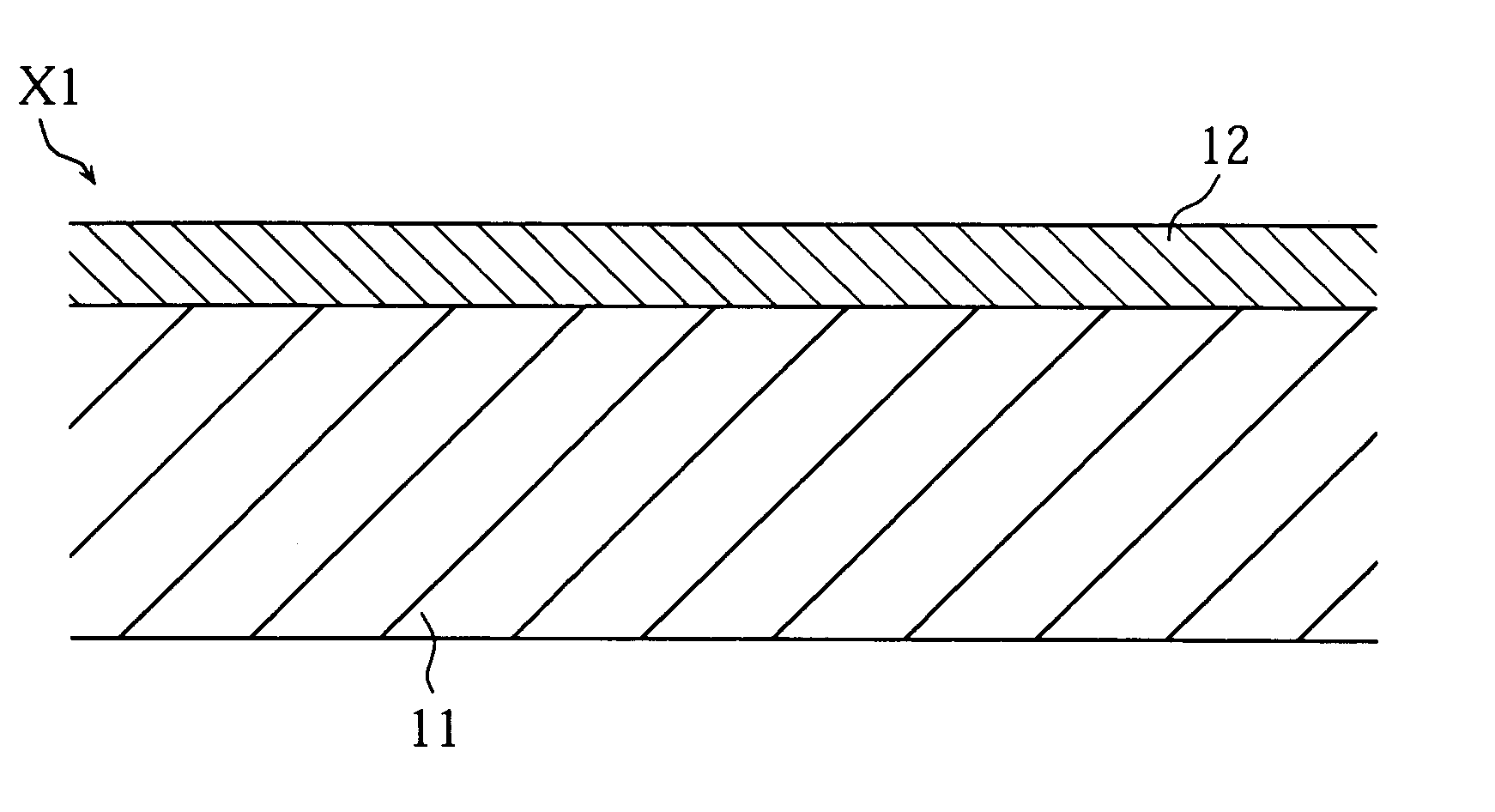
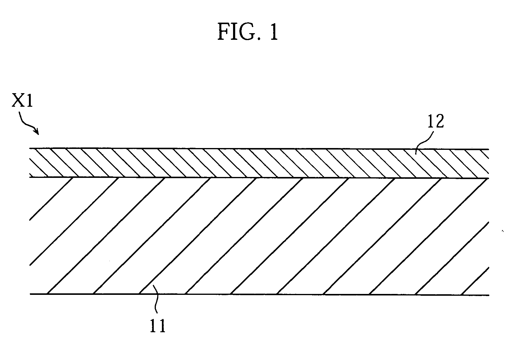
[0062] 40 recording medium substrates of the present example were manufactured as substrates having one of the structures described earlier with regard to the recording medium substrate X1. In the manufacture of each of the recording medium substrates of the present example, Ni80Fe20 was deposited by sputtering on a glass disk substrate (diameter 90 mm, thickness 1.2 mm), thus forming an NiFe layer of thickness 30 nm as a foundation film. In this sputtering, an NiFe alloy target (diameter 6 inches) was used. Moreover, in the sputtering, Ar gas was used as a sputter gas, the sputter gas pressure was set to 0.5 Pa, and the electrical discharge power was set to 1.0 kW. The same sputtering conditions were also used in other examples described hereinafter. The details of the makeup of the recording medium substrates of the present example are shown in Tables 1 to 4, together with those for the other examples.
example 2
[0063] 40 recording medium substrates of the present example were manufactured as substrates according to the recording medium substrate X1. In the manufacture of each of the recording medium substrates of the present example, Co80Fe20 was deposited by sputtering on a glass disk substrate (diameter 90 mm, thickness 1.2 mm), thus forming a CoFe layer of thickness 30 nm as a foundation film. In this sputtering, a CoFe alloy target (diameter 6 inches) was used.
example 3
[0064] 40 recording medium substrates of the present example were manufactured as substrates according to the recording medium substrate X1. In the manufacture of each of the recording medium substrates of the present example, first Ti was deposited by sputtering on a glass disk substrate (diameter 90 mm, thickness 1.2 mm), thus forming a Ti layer of thickness 5 nm as a bonding layer. In this sputtering, a Ti target (diameter 6 inches) was used. Next, Cu85Ni15 was deposited by sputtering, thus forming a CuNi layer of thickness 30 nm as a foundation film. In this sputtering, a CuNi alloy target (diameter 6 inches) was used.
PUM
| Property | Measurement | Unit |
|---|---|---|
| thickness | aaaaa | aaaaa |
| thickness | aaaaa | aaaaa |
| thickness | aaaaa | aaaaa |
Abstract
Description
Claims
Application Information
 - Generate Ideas
- Intellectual Property
- Life Sciences
- Materials
- Tech Scout
- Unparalleled Data Quality
- Higher Quality Content
- 60% Fewer Hallucinations
Browse by: Latest US Patents, China's latest patents, Technical Efficacy Thesaurus, Application Domain, Technology Topic, Popular Technical Reports.
© 2025 PatSnap. All rights reserved.Legal|Privacy policy|Modern Slavery Act Transparency Statement|Sitemap|About US| Contact US: help@patsnap.com


