
Liquid crystal display panel and method for producing the same

a liquid crystal display and display panel technology, applied in non-linear optics, instruments, optics, etc., can solve the problems of reducing the voltage retention rate, affecting the image quality, and affecting reliability, so as to achieve the effect of efficient production of liquid crystal display panels and thicker widths

Active Publication Date: 2006-01-19
SHARP KK
View PDF7 Cites 32 Cited by
  • Summary
  • Abstract
  • Description
  • Claims
  • Application Information

AI Technical Summary

Benefits of technology

[0027] In order to overcome the problems described above, preferred embodiments of the present invention provide: a method for efficiently producing a liquid crystal display panel whose reliability will not be degraded even if a portion (e.g., a sealing junction or transfer section) which under the conventional production methods will result in a seal pattern having a thicker width is formed in the liquid crystal display panel; and a liquid crystal display panel which is provided by such a production method.
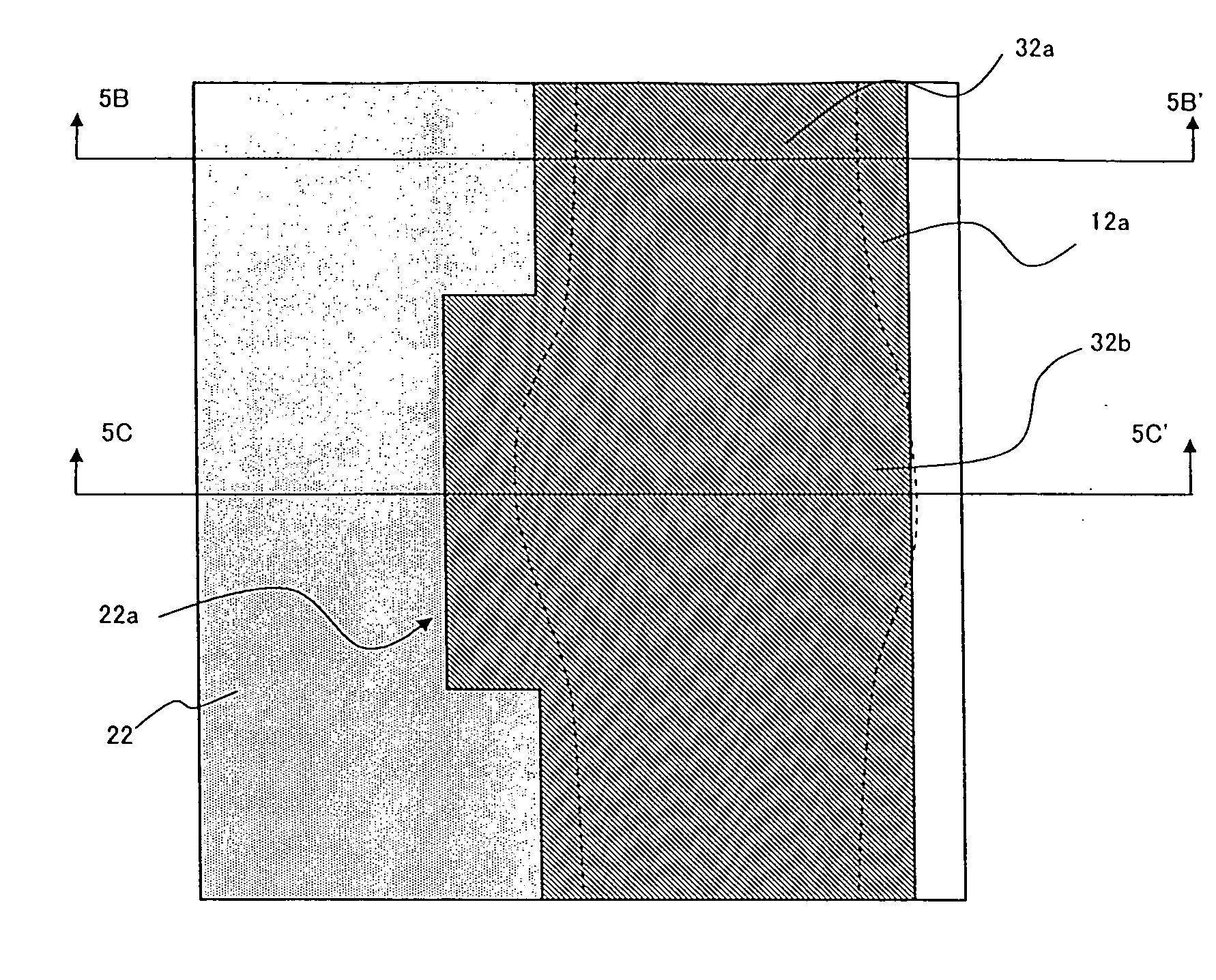
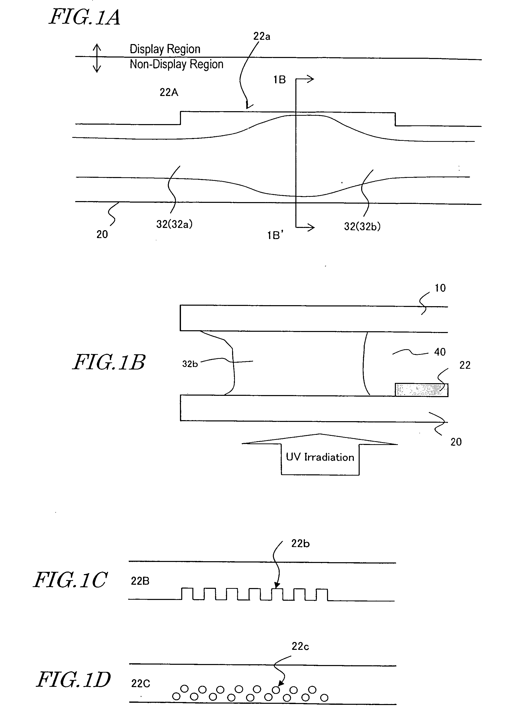
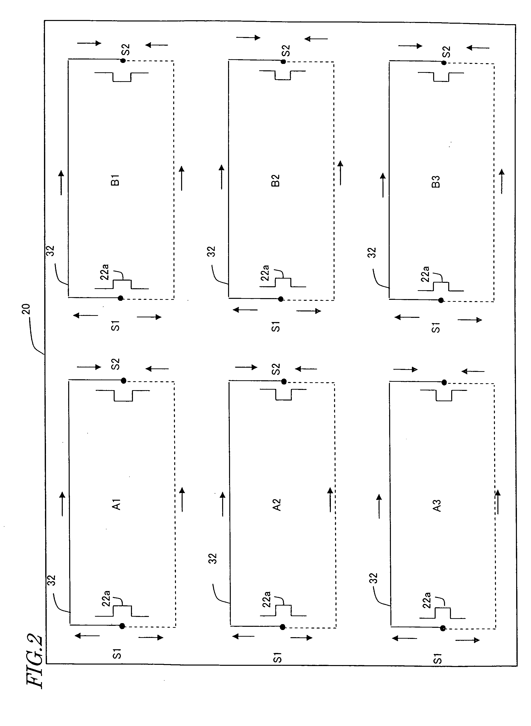
[0061] In accordance with a liquid crystal display panel production method of the present invention, a substrate including a light shielding layer which has a light-transmitting portion (recess or opening) at a position to become a junction of a sealant is used, and light irradiation is performed from the side of this substrate. As a result, insufficient sealant curing at the junction is prevented. Moreover, by providing a light-transmitting portion at a corner portion or a transfer section (e.g., a common transfer section) at which the width of the seal pattern is likely to become broadened, curing failure of the sealant at such a corner portion or transfer section can also be prevented. Thus, since a light-transmitting portion is provided only in a portion(s) of the light shielding layer at which the width of the seal pattern is expected to become thick, the width of the non-display region can be kept narrow. Furthermore, by providing a light shielding layer on another substrate (at a position opposing the position at which the light-transmitting portion is provided on the first substrate), the original purpose of the light shielding layer, i.e., prevention of light leakage, will not be undermined.
[0063] By using a color filter substrate as the aforementioned substrate, damage to the TFTs due to UV can be reduced. Furthermore, it becomes possible to omit a mask to be used for protecting the TFTs in the light irradiation process. By performing light irradiation also from the TFT substrate side, the irradiation time required for the curing can be reduced.

Problems solved by technology

If light shielding is insufficient, black displaying quality is degraded, thus substantially affecting the image quality.
As a result, the uncured component of the photocurable resin may elute into the liquid crystal material, thus causing deterioration in reliability, e.g., lowering of the voltage retention rate of the liquid crystal display panel mainly due to ionic components, and occurrence of orientation defects.
However, this method cannot cope with the above problem once the width of the sealing junction exceeds about 1.4 times the aforementioned value, as is also pointed out in Japanese Laid-Open Patent Publication No. 2002-122870.
In such cases, there is a problem in that a sealing portion 32t will remain on the TFT mother substrate 10, which will stick to a fragment of the CF mother substrate 20 to be removed, thus making it impossible to remove the fragment.
Such a seal pattern drawing apparatus will inevitably be large in size, and hence increase the production cost of the display panel.

Method used


Image

  • Liquid crystal display panel and method for producing the same
  • Liquid crystal display panel and method for producing the same
  • Liquid crystal display panel and method for producing the same

Examples


Embodiment Construction

[0092] Hereinafter, a liquid crystal display panel according to an embodiment of the present invention and a method for producing the same will be described, with reference to the accompanying drawings.

[0093] As shown in FIGS. 1A and 1B, a liquid crystal display panel according to an embodiment of the present invention includes: a TFT substrate 10, a color filter substrate 20, a liquid crystal layer 40 provided between the TFT substrate 10 and the color filter substrate 20, and a sealing portion 32 surrounding the liquid crystal layer 40. The liquid crystal display panel has a display region and a non-display region surrounding the display region. The color filter substrate 20 has a first light shielding layer 22A, which is provided within the non-display region, at an end closer to the display region. The first light shielding layer 22A has a recess (light-transmitting portion) 22a provided near the outer boundary. The width of the sealing portion 32 is allowed to become wider at ...


PUM


Abstract

The method of the present invetion includes the steps of: (A) providing a first substrate, and a second substrate, wherein the first substrate includes a first light shielding layer provided within a non-display region, the first light shielding layer including a light-transmitting portion provided near an outer boundary of the first light shielding layer, the light-transmitting portion comprising a recess or an opening; (B) drawing a seal pattern with a sealant, the seal pattern being drawn outside the first light shielding layer so as to surround the display region, comprising the substeps of: (B1) beginning application of the sealant near the light-transmitting portion, (B2) applying the sealant along an outer periphery of the first light shielding layer, and (B3) forming a junction with the sealant having been applied near the light-transmitting portion; (C) applying a liquid crystal material within the display region surrounded by the sealant; (D) attaching the first substrate and the second substrate; and (E) performing light irradiation from the first substrate side to cure the sealant.

Description

BACKGROUND OF THE INVENTION [0001] 1. Field of the Invention [0002] The present invention relates to a liquid crystal display panel and a method for producing the same. More particularly, the present invention relates to a method for producing a liquid crystal display panel by using one drop filling technique, and a liquid crystal display panel suitable for such a production method. [0003] 2. Description of the Related Art [0004] In recent years, as liquid crystal display panels become larger in size, it is becoming more common to adopt a so-called one drop filling technique as a method for forming a liquid crystal layer between a pair of substrates, instead of the conventionally-used vacuum injection technique. [0005] A process of producing a liquid crystal display panel using a vacuum injection technique comprises the following steps. [0006] (a1) On one of a pair of substrates (which typically are a color filter substrate and a TFT substrate) for composing a liquid crystal display...

Claims


Application Information

Patent Timeline
IPC IPC(8): G02F1/1333G02F1/1339
CPCG02F1/133351G02F2001/13415G02F1/1339G02F1/13415
Inventor YAMADA, NAOSHIYAMAGUCHI, HIDEHIKOTSUBATA, TOSHIHIDEKUROZUMI, YUKIOTSUJI, MASAYUKI
Owner SHARP KK
Learn More