Resist pattern forming method, substrate processing method, and device manufacturing method
- Summary
- Abstract
- Description
- Claims
- Application Information
AI Technical Summary
Benefits of technology
Problems solved by technology
Method used
Image

Examples
Embodiment Construction
[0024] Preferred embodiments of the present invention will now be described with reference to the attached drawings.
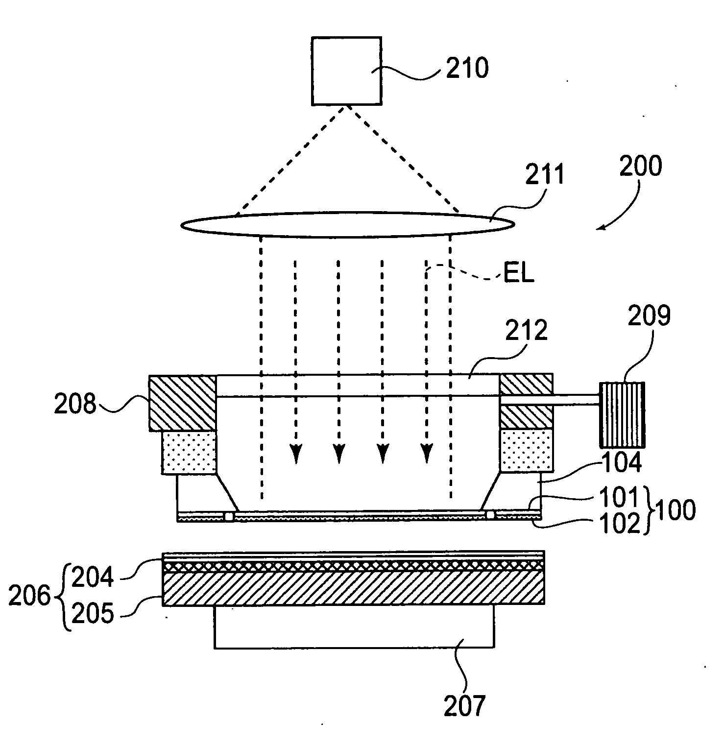
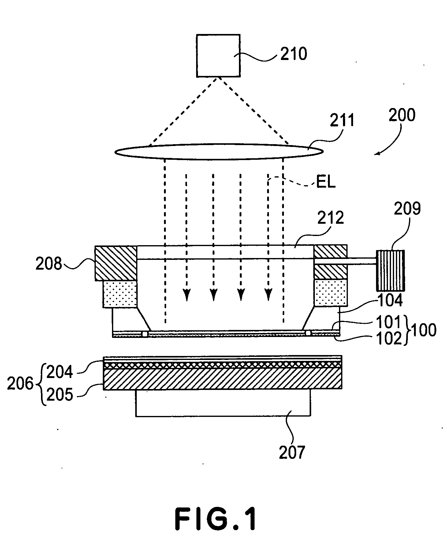
[0025]FIG. 1 is a schematic view of a general structure of an exposure apparatus into which a resist pattern forming method according to an embodiment of the present invention is incorporated. In FIG. 1, denoted at 200 is a near-field exposure apparatus that comprises a pressure adjusting container 208, an exposure light source 210, a stage 207, and a pressure adjusting device 209 for adjusting the pressure inside the pressure adjusting container 208.
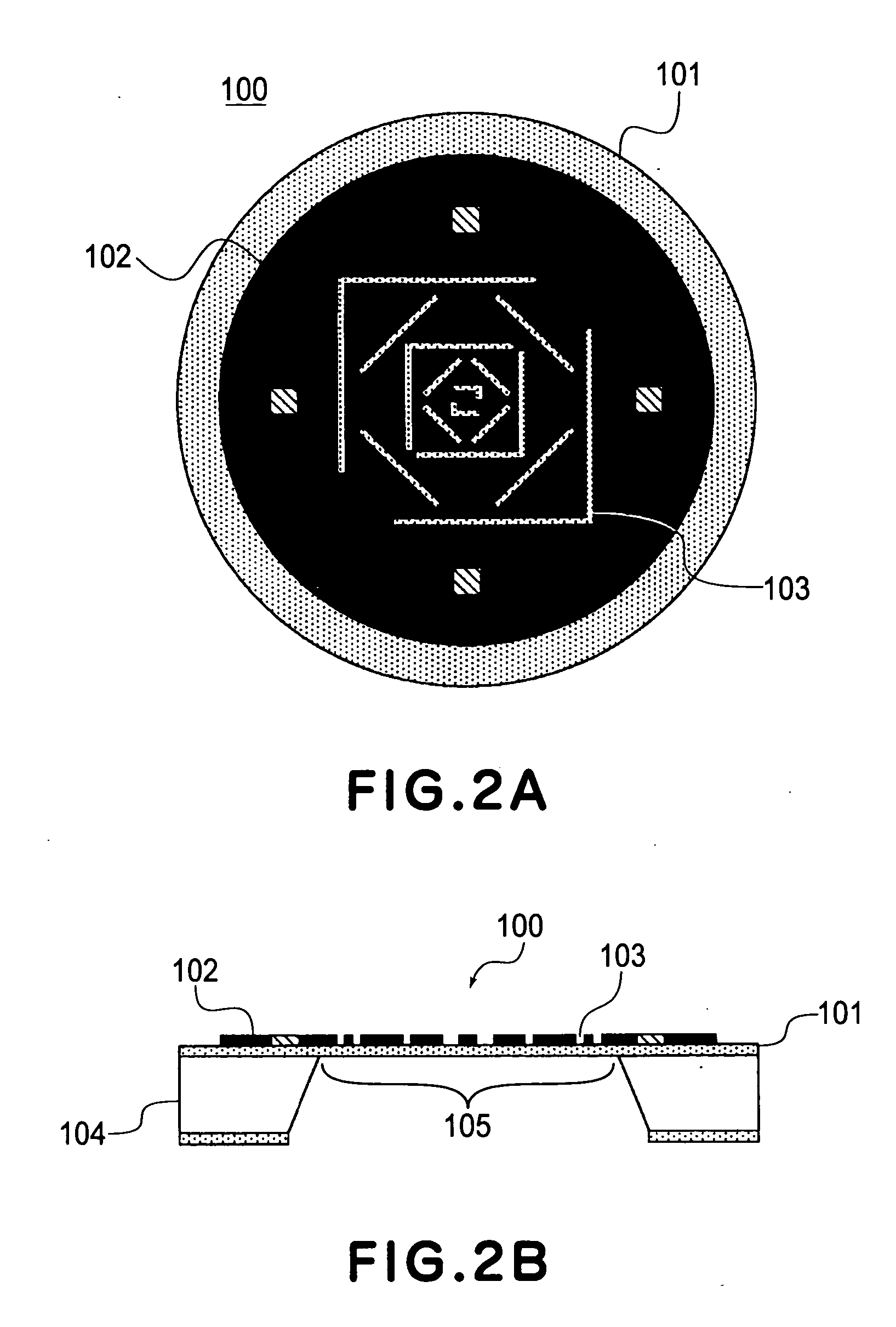
[0026] Denoted at 100 in FIG. 1 is an exposure mask which is attached to the bottom of the pressure adjusting container 208. As best seen in FIGS. 2A and 2B, this exposure mask 100 comprises a mask supporting member 104, a mask base material 101 and a light blocking film 102. The light blocking film 102 is formed to be held by the mask base material 101 which is a thin-film holding member made of an elastic (resilient) m...
PUM
 Abstract
Description
Claims
Application Information
 - R&D
- Intellectual Property
- Life Sciences
- Materials
- Tech Scout
- Unparalleled Data Quality
- Higher Quality Content
- 60% Fewer Hallucinations
Browse by: Latest US Patents, China's latest patents, Technical Efficacy Thesaurus, Application Domain, Technology Topic, Popular Technical Reports.
© 2025 PatSnap. All rights reserved.Legal|Privacy policy|Modern Slavery Act Transparency Statement|Sitemap|About US| Contact US: help@patsnap.com