
A kind of electroplating method for printed circuit board

A printed circuit board and electroplating gold technology, which is applied in the field of electroplating gold, can solve the problems of poor coverage of non-gold-plated areas, poor gold-plating quality, poor dry film adhesion, etc., and achieve the goal of improving the quality of printed circuit boards and line width accuracy Effect

Active Publication Date: 2018-10-23
南通深南电路有限公司
View PDF2 Cites 0 Cited by
  • Summary
  • Abstract
  • Description
  • Claims
  • Application Information

AI Technical Summary

Problems solved by technology

[0011] In the above process, the adhesion of the dry film is poor, and the coverage of the non-gold-plated area is not strict, resulting in the problem of gold-plating bleeding and poor gold-plating quality

Method used


Image

  • A kind of electroplating method for printed circuit board

Examples


Embodiment Construction

[0025] The following will clearly and completely describe the technical solutions in the embodiments of the present invention with reference to the accompanying drawings of the embodiments of the present invention. Obviously, the described embodiments are only some, not all, embodiments of the present invention. Based on the embodiments of the present invention, all other embodiments obtained by persons of ordinary skill in the art without creative efforts fall within the protection scope of the present invention.

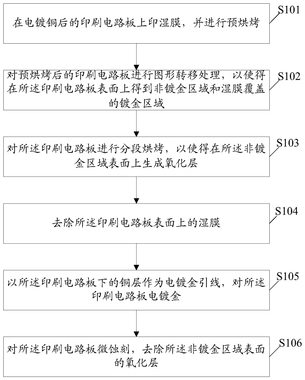
[0026] An embodiment of the present invention provides a gold electroplating method for a printed circuit board, which is used to improve the line width precision at the junction of a gold-plated area and a non-gold-plated area, and improve the gold-plating quality.

[0027] Below with specific embodiment, the present invention is described in detail:

[0028] see figure 1 , figure 1 The schematic flow chart of the electroplating gold method for printed circuit b...


PUM


Abstract

The invention discloses an electrogilding method for a printed circuit board, and aims at solving the problem in electrogilding cementation, improving the aligning precision of a connecting position between a gilding area and a non-gilding area, and improving the quality of the printed circuit board. The method comprises that a wet film is printed on the printed circuit board after electrocoppering and pre-baked; pattern transfer is carried out on the pre-baked printed circuit board, so that a non-gilding area and a gilding area covered by the wet film are obtained at the surface of the printed circuit board; the printed circuit board is baked in segment, so that an oxide layer is formed at the surface of the non-gilding area; the wet film at the surface of the printed circuit board is removed; a copper layer under the printed circuit board serves as an electrogilding lead to electrogild the printed circuit board; and micro-etching is carried out on the printed circuit board to remove the oxide layer at the surface of the non-gilding area.

Description

technical field [0001] The invention relates to the technical field of printed circuit board (PCB, Printed Circuit Board) production, in particular to an electroplating method for printed circuit boards. Background technique [0002] At present, the PCB surface gold plating process may include the following steps: [0003] A1. Make the graphics and gold-plated leads of the gold-plated area on the PCB; [0004] A2. Paste the dry film on the non-gold-plated area, and then gold-plate the gold-plated area; [0005] A3. Make non-gold-plated area graphics; [0006] A4. Other surface coating operations. [0007] In the above process, the gold-plated area on the PCB is first made for the first graphics, and then a dry film is attached to the non-gold-plated area for protection, and gold-plated on the gold-plated area without a dry film, and then the non-gold-plated area is removed. Dry film, making graphics on non-gold-plated areas, for second graphics. Two successive graphic p...

Claims


Application Information

Patent Timeline
Patent Type & Authority Patents(China)
IPC IPC(8): H05K3/24
Inventor 丁大舟刘宝林郭长峰缪桦
Owner 南通深南电路有限公司
Learn More