
Capacitor assemblies

Active Publication Date: 2005-12-29
INFINEON TECH AG
View PDF25 Cites 175 Cited by
  • Summary
  • Abstract
  • Description
  • Claims
  • Application Information

AI Technical Summary

Benefits of technology

[0007] By way of introduction only, a capacitor assembly and method for the fabricating capacitor assemblies are described. The present invention provides a capacitor arrangement and simple method for fabricating a capacitor arrangement, which makes it possible in particular to fabricate capacitor arrangements having a high quality and a high linearity and / or a high capacitance per unit area.
[0008] The present invention is based, at least in part, on the consideration of technological development to provide the highest possible capacitance per unit area. This may be achieved, for example, by selecting dielectrics whose dielectric constant is as high as possible. A minimum permissible thickness, and therefore, also the maximum capacitance per unit area are determined by the product requirements relating to service life and dielectric strength. By way of example, with a thickness of approximately 45 nm of silicon nitride SiN, a capacitance of approx. 1.30 fF / μm2 (Femtofarad per square micrometer) may be achieved with a service life of 15 years, 2.3 mm 2 total surface area in the product and an operating voltage of 3.6 V. A further reduction in the thickness may lead to product failures within the 15 years on which the product is based. Higher overall capacitances lead to further demands for area in the product, and therefore, to higher chip costs.
[0009] The invention is also based, at least in part, on the consideration that the outlay involved in patterning each individual electrode is a factor that may limit the number of electrodes arranged between two metallization layers from being increased. This outlay increases linearly in relation to the number of electrodes unless additional measures are taken. Therefore, in a method according to one embodiment of the invention, at least one center electrode layer and a covering dielectric layer are arranged between the base dielectric layer and the covering electrode layer. The covering electrode layer and the center electrode layer are patterned using a first lithography method, and then, the pre patterned covering electrode layer and the base electrode layer are patterned using a second lithography method. Therefore, a method according to the invention may use just two lithography methods for three electrodes. The linear relationship between the number of electrodes and the number of lithography methods used to pattern the capacitor arrangement is broken. As a result, the number of lithography and etching steps involved in the process is considerably reduced. The more electrodes are stacked on top of one another for a capacitor arrangement, the more manifest this effect becomes.

Problems solved by technology

1.30 fF / μm2 (Femtofarad per square micrometer) may be achieved with a service life of 15 years, 2.3 mm 2 total surface area in the product and an operating voltage of 3.6 V. A further reduction in the thickness may lead to product failures within the 15 years on which the product is based.
Higher overall capacitances lead to further demands for area in the product, and therefore, to higher chip costs.

Method used


Image

  • Capacitor assemblies
  • Capacitor assemblies
  • Capacitor assemblies

Examples


Embodiment Construction

[0079] Capacitor assemblies will now be described more fully with reference to the accompanying drawings. In each of the following figures, components, features and integral parts that correspond to one another each have the same reference number. The drawings of the figures are not true to scale.

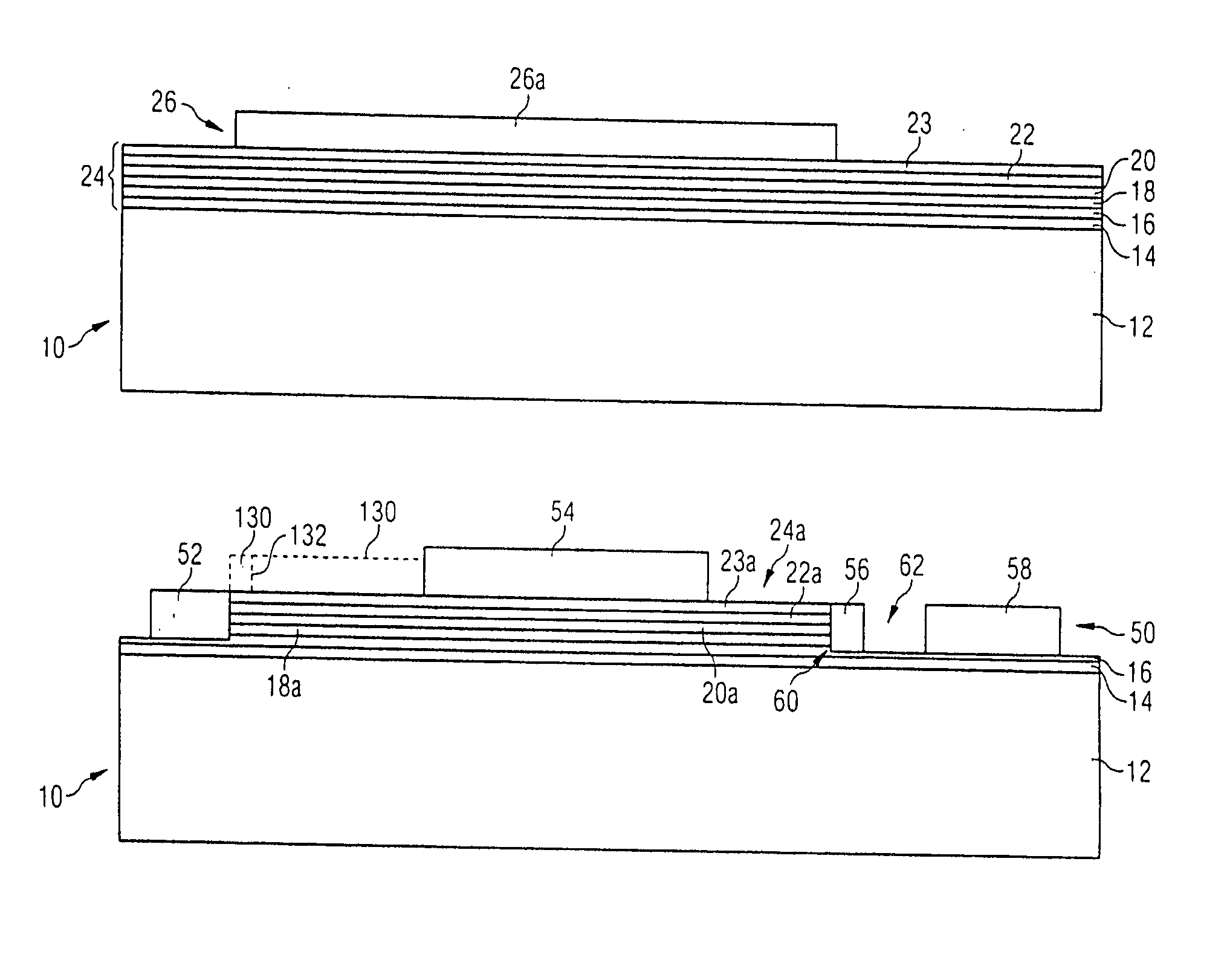
[0080]FIG. 1 shows an intermediate stage in the fabrication of a capacitor arrangement 10 that is arranged on a dielectric layer 12. The dielectric layer 12 forms a dielectric between various interconnects of a metallization layer in the interior of an integrated circuit arrangement. By way of example, the dielectric layer 12 has a thickness of 300 nm and consist of silicon dioxide.

[0081] A base electrode layer is applied to the dielectric layer 12, for example by sputtering. In the exemplary embodiment, the electrode layers include titanium nitride TiN. The electrode layers have a thickness of, for example, in each case 50 nm.

[0082] After a base electrode layer 14 has been applied, a ba...


PUM


Abstract

A method for fabricating a capacitor arrangement which includes at least three electrodes is described. The capacitor arrangement is fabricated using a number of lithography methods that is smaller than the number of electrodes. A capacitor arrangement extending over more than two or more interlayers between metallization layers has a high capacitance per unit area and can be fabricated in a simple way is also described. The circuit arrangement has a high capacitance per unit area and can be fabricated in a simple way. An electrode layer is first patterned using a dry-etching process and residues of the electrode layer are removed using a wet-chemical process, making it possible to fabricate capacitors with excellent electrical properties.

Description

PRIORITY AND CROSS REFERENCE TO RELATED APPLICATION [0001] This application is a continuation of International Application No. PCT / DE03 / 03933 filed Nov. 27, 2003, which claims priority to German application 102 60 352.9 filed Dec. 20, 2002, both of which are incorporated herein in their entirety by reference.BACKGROUND [0002] 1. Field of the Invention [0003] The present invention relates to the field of the integrated capacitor assemblies and fabrication thereof. In particular, the present invention relates to a capacitor arrangement having a layer stack. [0004] 2. Description of the Related Art [0005] Integrated circuit arrangements having capacitors, known as MIM (metal insulator metal) capacitors, may be used in integrated circuit arrangements. Electrode layers, or the electrodes, in these capacitors are not necessarily produced from a metal or a metal alloy. For example, there are electrodes made from doped polysilicon. The electrodes usually have a resistivity of less than 10-3...

Claims


Application Information

Patent Timeline
IPC IPC(8): H01L27/08
CPCH01L27/0805
Inventor BACHMANN, JENSFOSTE, BERNDGOLLER, KLAUSKRIZ, JAKOB
Owner INFINEON TECH AG
Learn More