
Adhesion and/or encapsulation of silicon carbide-based semiconductor devices on ceramic substrates

a technology of silicon carbide and semiconductors, applied in semiconductor devices, semiconductor/solid-state device details, electrical apparatus, etc., can solve the problems of rapid temperature change, inability to deploy lateral sic devices (which require back-side electrical isolation) in high-temperature environments,

Inactive Publication Date: 2005-12-29
MICROSEMI CORP
View PDF19 Cites 5 Cited by
  • Summary
  • Abstract
  • Description
  • Claims
  • Application Information

AI Technical Summary

Benefits of technology

The borosilicate glass encapsulant provides a stable, electrically insulating, and non-conductive layer that protects SiC devices and circuits from mechanical and thermal stress, enabling their deployment in extreme environments without degradation, and ensures the thermal and mechanical stability of the hybrid structure, allowing for high-temperature operation without limitations.

Problems solved by technology

Without this technology, lateral SiC devices (which require back-side electrical isolation) cannot be deployed in environments of high temperature, or rapid temperature changes.

Method used


Image

  • Adhesion and/or encapsulation of silicon carbide-based semiconductor devices on ceramic substrates
  • Adhesion and/or encapsulation of silicon carbide-based semiconductor devices on ceramic substrates

Examples


example 1

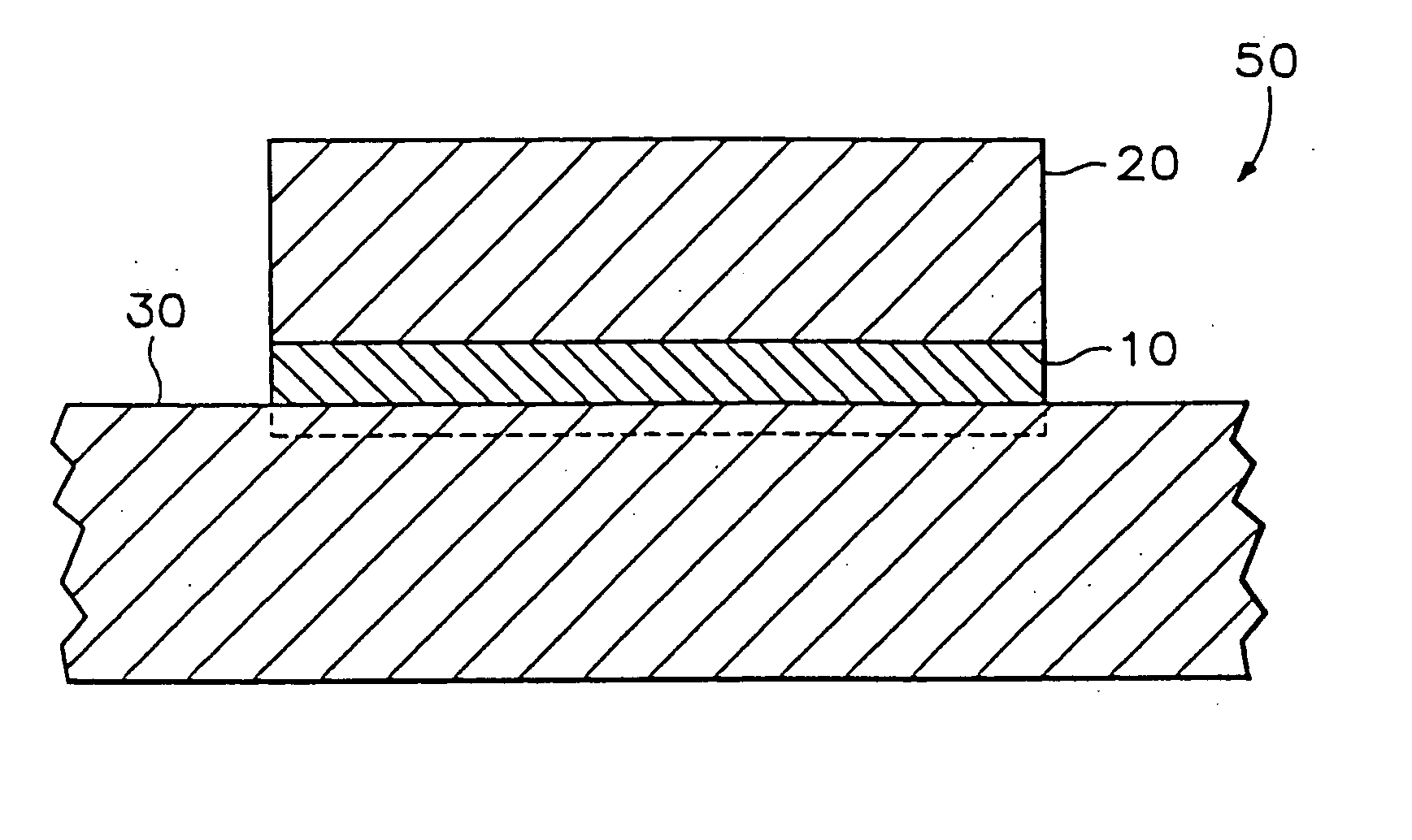
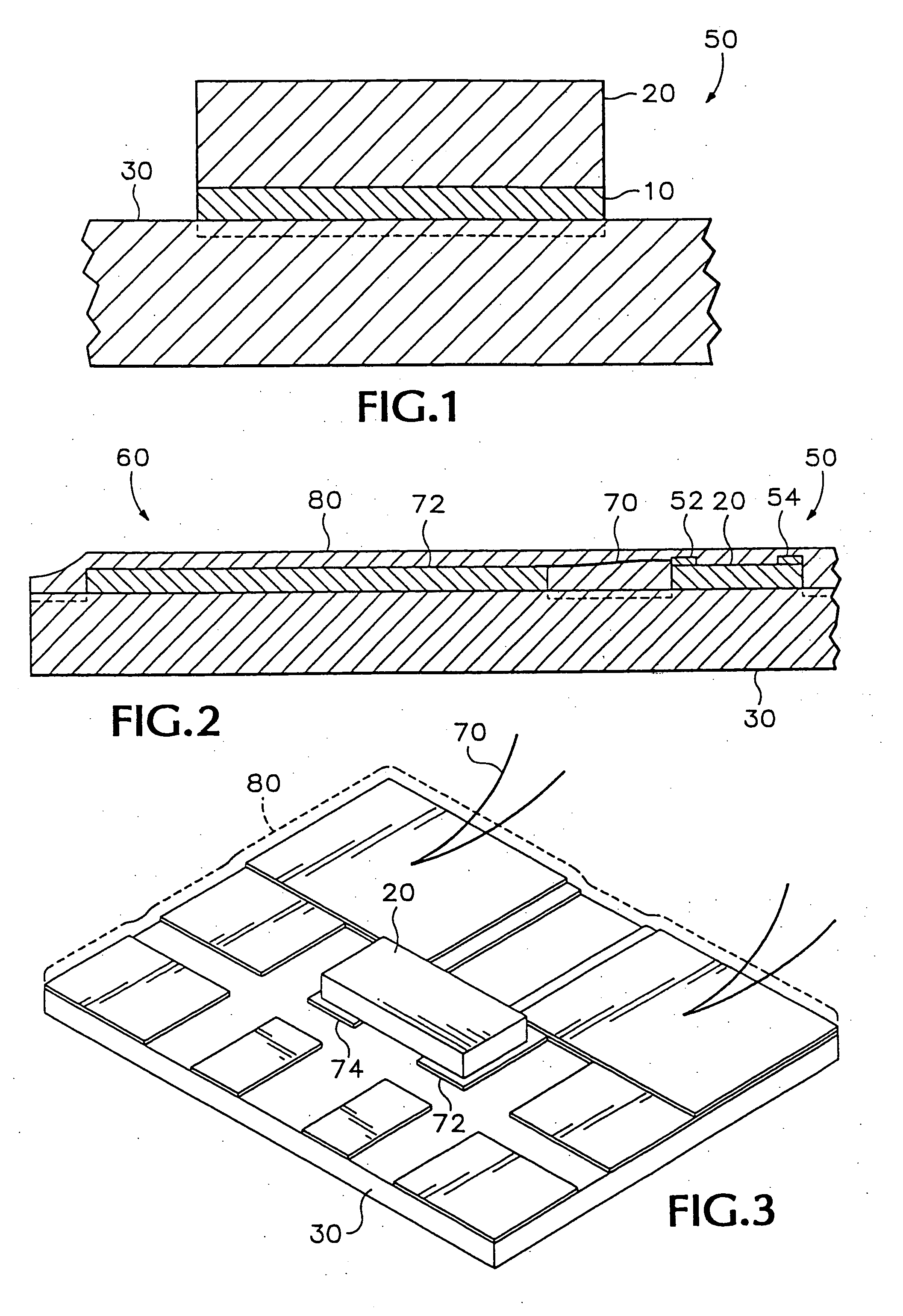
[0062] As depicted in FIG. 1, a bonding material 10, comprising borosilicate glass (composition=30 to 50 weight % B2O3+70 to 50 weight % SiO2), was produced and was employed as a high temperature, shock immune adhesive to bond an SiC wafer 20 to AlN die 30. The resulting structure is a SiC semiconductor on ceramic substrate 50.

[0063] The bonding material 10 was initially composed of finely ground and mixed powders of: (a) unreacted constituent oxides, or (b) reacted mixture. The adhesive was applied to one of the bonding surfaces (preferably the bottom side of the SiC wafer) as a dry powder, but can also be applied in the form of a slurry. In slurry form, all vaporizable slurry constituents (e.g. water) should be baked off before performing the bonding process.

[0064] The surfaces to be bonded (at least one of them coated with the dried adhesive) were placed together, and shift pressure was applied. The process is thermally activated by transferring the assembly from ambient air to...

example 2

[0072] The protective attributes of the stable encapsulating layer of this invention were experimentally determined, as follows:

[0073] Referring now to FIG. 2, a portion of a tungsten (W) wire 70, which oxidizes easily, was connected to a metal bond pad 52 on an ohmic contact on the SiC chip and to the metal bond pad 72 on the AlN substrate. The assembly 50 as well as the wire 70 and pads 52, 54, 72 were then encapsulated within an encapsulating layer 80, on the AlN die 30, following the temperature ramping procedure described in Example 1. Then the encapsulated assembly was heated to 1200° C. in air for 30 minutes. As a control, a portion of the tungsten wire 70 was not encapsulated by encapsulating layer 80. In general, elemental tungsten forms two types of oxides WO2 (purple) and WO3 (yellow). The result of this experiment was as follows: (1) the exposed portion of the tungsten wire 20 was oxidized and formed a yellow, non-conductive powder (WO3), (2) the encapsulated portion of...


PUM

PropertyMeasurementUnit
temperaturesaaaaaaaaaa
temperatureaaaaaaaaaa

Abstract

A SiC die with Os and / or W / WC / TiC contacts and metal conductors is encapsulated either alone or on a ceramic substrate using a borosilicate (BSG) glass that is formed at a temperature well below upper device operating temperature limits but serves as a stable protective layer above the operating temperature (over 1000° C., preferably >1200° C.). The glass is preferably 30-50% B2O3 / 70-50% SiO2, formed by reacting a mixed powder, slurry or paste of the components at 460°-1000° C. preferably about 700° C. The die can be mounted on the ceramic substrate using the BSG as an adhesive. Metal conductors on the ceramic substrate are also protected by the BSG. The preferred ceramic substrate is AlN but SiC / AlN or Al2 03 can be used.

Description

RELATED APPLICATION DATA [0001] This application is a continuation of copending U.S. patent application Ser. No. 10 / 016,578, filed Nov. 1, 2001, now U.S. Pat. No. 6,911,714, to be issued Jun. 28, 2005, which is a division of U.S. patent application Ser. No. 09 / 351,106, filed Jul. 6, 1999, now U.S. Pat. No. 6,319,757, issued Nov. 20, 2001, which claims priority from U.S. Provisional Application Ser. No. 60 / 092,039, filed Jul. 8, 1998.BACKGROUND OF THE INVENTION [0002] This invention relates generally to the adhesion and / or encapsulation of semiconductor devices or circuits on ceramic substrates, and more particularly to the adhesion and / or encapsulation of silicon carbide semiconductors with metal or alloy contacts and conductors, and metal circuits on AlN substrates. [0003] SiC-based semiconductor devices possess tremendous advantages for high temperature and high power solid state electronics. In addition, these devices offer potential advantages for high frequency and logic circui...

Claims


Application Information

Patent Timeline
Patent Type & Authority Applications(United States)
IPC IPC(8): H01L21/04H01L21/58H01L23/29H01L29/15
CPCH01L21/0485H01L21/0495H01L23/291H01L24/83H01L2224/8319H01L2224/8385H01L2924/01005H01L2924/01013H01L2924/01015H01L2924/01029H01L2924/0104H01L2924/01042H01L2924/01046H01L2924/01047H01L2924/01052H01L2924/01073H01L2924/01074H01L2924/01075H01L2924/01077H01L2924/01078H01L2924/01079H01L2924/01082H01L2924/01327H01L2924/07802H01L2924/09701H01L2924/10329H01L2924/13055H01L2924/13091H01L2924/14H01L2924/19043H01L2924/3025H01L2924/13063H01L24/29H01L2224/2919H01L2924/01006H01L2924/01019H01L2924/01021H01L2924/01023H01L2924/01024H01L2924/01033H01L2924/01041H01L2924/01043H01L2924/01044H01L2924/01045H01L2924/01072H01L2924/01076H01L2924/0665Y10S438/931H01L2924/1306H01L2924/1301H01L2924/1305H01L2924/12032H01L2924/00H01L2924/3512H01L2924/12036H01L2924/15787H01L2924/351
Inventor PARSONS, JAMES D.KWAK, B. LEO
Owner MICROSEMI CORP
Learn More