Mask blank, phase shift mask manufacturing method and template manufacturing method
- Summary
- Abstract
- Description
- Claims
- Application Information
AI Technical Summary
Benefits of technology
Problems solved by technology
Method used
Image
Examples
embodiment 1
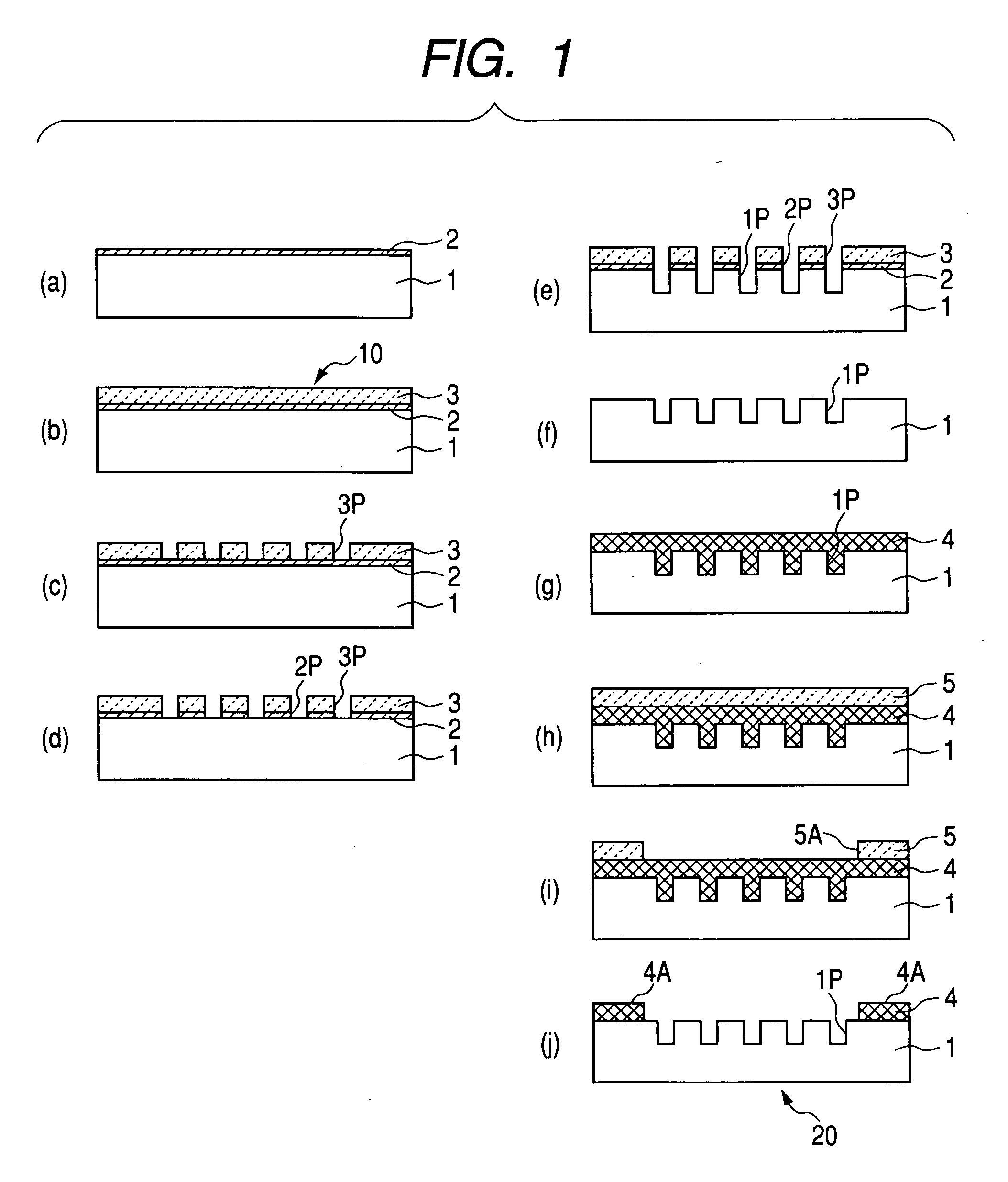
[0047] A method of manufacturing a phase shift mask according to an embodiment 1 will be described with reference to FIG. 1.
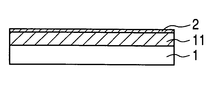
[0048] First of all, a chromium nitride film (a very thin film) 2 was formed in a thickness of 5 nm on a transparent substrate (hereinafter referred to as a quartz substrate) 1 by using a sputtering method, and the quartz substrate 1 having the very thin chromium nitride film 2 for a processing shown in (a) was fabricated. The chromium nitride film 2 was fabricated in a reactive sputtering film formation using chromium as a sputter target and a nitrogen gas as a sputter gas. The thickness of the very thin chromium nitride film 2 was measured by an optical film thickness meter. Referring to the accuracy of a measured value, moreover, the substrate 1 and the chromium nitride film 2 were broken to observe and confirm a sectional TEM (a tunnel electron microscope) image.
[0049] Next, an electron beam resist film 3 (manufactured by Fuji Film Arch (FFA) Co., Ltd.: T...
embodiment 2
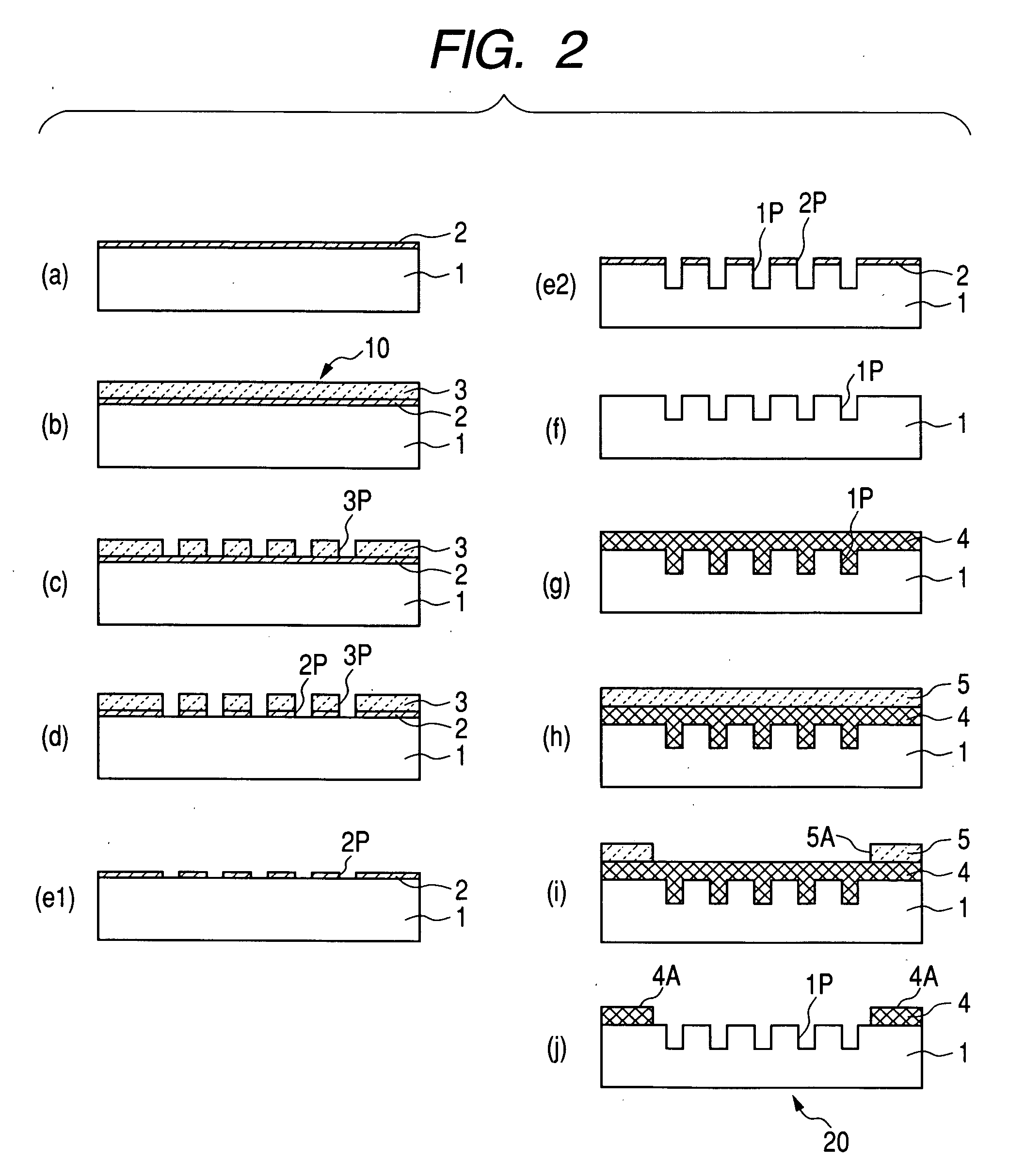
[0060] An embodiment 2 will be described with reference to FIG. 2. The embodiment 2 shows the case in which a resist pattern 3P to be a primary pattern is removed.
[0061] In the embodiment, the thickness of a chromium nitride film 2 to be formed on a quartz substrate 1 was first set to be 40 nm. Other portions were the same as those in the Embodiment 1. The thickness of the chromium nitride film 2 was different from that in the embodiment 1. In embodiment, however, the chromium nitride film 2 was processed by etching for 120 seconds including an over-etching time (a just etching time: 100 seconds) on the same chromium nitride dry etching condition as that in the embodiment 1. Also in this case, in the same manner as in the embodiment 1, the processing can be carried out in a sufficiently shorter time than a normal time required for etching a light shielding film containing chromium.
[0062] The same processings as in the embodiment 1 were carried out from (a) to (d). After the end of...
embodiment 3
[0067] A third embodiment will be described with reference to FIG. 3.
[0068] A chromium nitride film 2 was used for a very thin film in the same manner as in the embodiment 1. The thickness of the chromium nitride film 2 was set to be 5 nm in the same manner as in the embodiment 1. Steps (a) to (e) were the same manner as those in the embodiment 1. At the step (e), the dry etching processing of a quartz substrate 1 was ended and only a resist pattern 3P (a primary pattern) was then removed. In a state in which a very thin chromium nitride pattern 2P (a secondary pattern) was left as shown in (f), a normal light shielding film 4 was formed as shown in (g). Consequently, a step of removing the very thin chromium nitride film 2 can be omitted so that a great advantage can be obtained in the process.
[0069] Also in the embodiment, subsequently, selective etching using a resist 5 was carried out as shown in steps (h) to (j) in the same manner as in the embodiments 1 and 2. Consequently, ...
PUM
 Abstract
Description
Claims
Application Information
 - R&D
- Intellectual Property
- Life Sciences
- Materials
- Tech Scout
- Unparalleled Data Quality
- Higher Quality Content
- 60% Fewer Hallucinations
Browse by: Latest US Patents, China's latest patents, Technical Efficacy Thesaurus, Application Domain, Technology Topic, Popular Technical Reports.
© 2025 PatSnap. All rights reserved.Legal|Privacy policy|Modern Slavery Act Transparency Statement|Sitemap|About US| Contact US: help@patsnap.com


